25F1024AN 查看數據表(PDF) - Unspecified
零件编号
产品描述 (功能)
生产厂家
25F1024AN Datasheet PDF : 20 Pages
| |||
2. Functional Description
The AT25F1024A is designed to interface directly with the synchronous serial peripheral inter-
face (SPI) of the 6800 type series of microcontrollers.
The AT25F1024A utilizes an 8-bit instruction register. The list of instructions and their operation
codes are contained in Table 2-1. All instructions, addresses, and data are transferred with the
MSB first and start with a high-to-low transition.
Write is defined as program and/or erase in this specification. The following commands, Pro-
gram, Sector Erase, Chip Erase, and WRSR are write instructions for AT25F1024A.
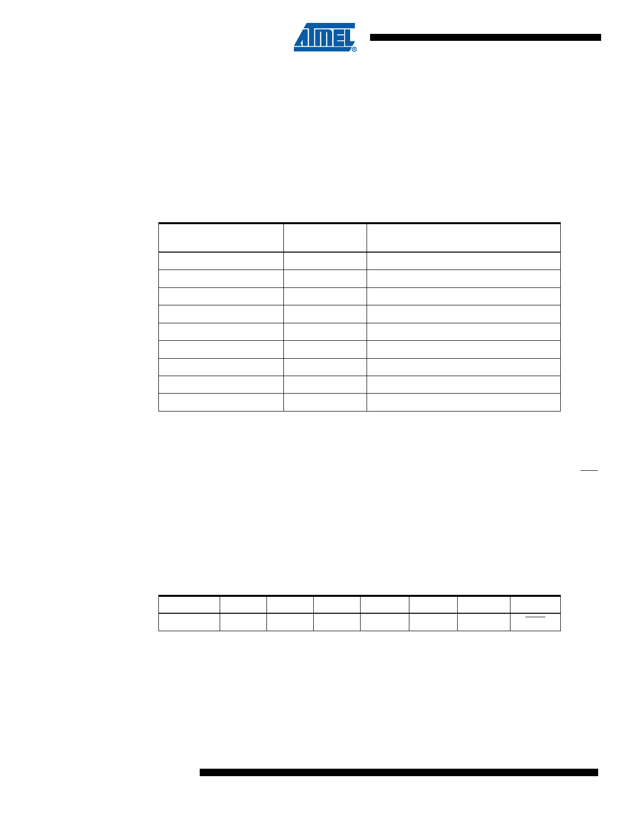
Table 2-1. Instruction Set for the AT25F1024A
Instruction Name
Instruction
Format
Operation
WREN
0000 X110
Set Write Enable Latch
WRDI
0000 X100
Reset Write Enable Latch
RDSR
0000 X101
Read Status Register
WRSR
0000 X001
Write Status Register
READ
0000 X011
Read Data from Memory Array
PROGRAM
0000 X010
Program Data into Memory Array
SECTOR ERASE
0101 X010
Erase One Sector in Memory Array
CHIP ERASE
0110 X010
Erase All Sectors in Memory Array
RDID
0001 X101
Read Manufacturer and Product ID
WRITE ENABLE (WREN): The device will power up in the write disable state when VCC is
applied. All write instructions must therefore be preceded by the WREN instruction.
WRITE DISABLE (WRDI): To protect the device against inadvertent writes, the WRDI instruc-
tion disables all write commands. The WRDI instruction is independent of the status of the WP
pin.
READ STATUS REGISTER (RDSR): The RDSR instruction provides access to the status regis-
ter. The Ready/Busy and write enable status of the device can be determined by the RDSR
instruction. Similarly, the Block Write Protection bits indicate the extent of protection employed.
These bits are set by using the WRSR instruction. During internal write cycles, all other com-
mands will be ignored except the RDSR instruction.
Table 2-2.
Bit 7
WPEN
Status Register Format
Bit 6
Bit 5
Bit 4
X
X
X
Bit 3
BP1
Bit 2
BP0
Bit 1
WEN
Bit 0
RDY
8 AT25F1024A
3346G–SFLSH–7/07
Share Link: 