ECP200G 查看數據表(PDF) - Unspecified
零件编号
产品描述 (功能)
生产厂家
ECP200G Datasheet PDF : 7 Pages
| |||
AH312
2 Watt, High Linearity InGaP HBT Amplifier
The Communications Edge TM
Product Information
Typical Device Data
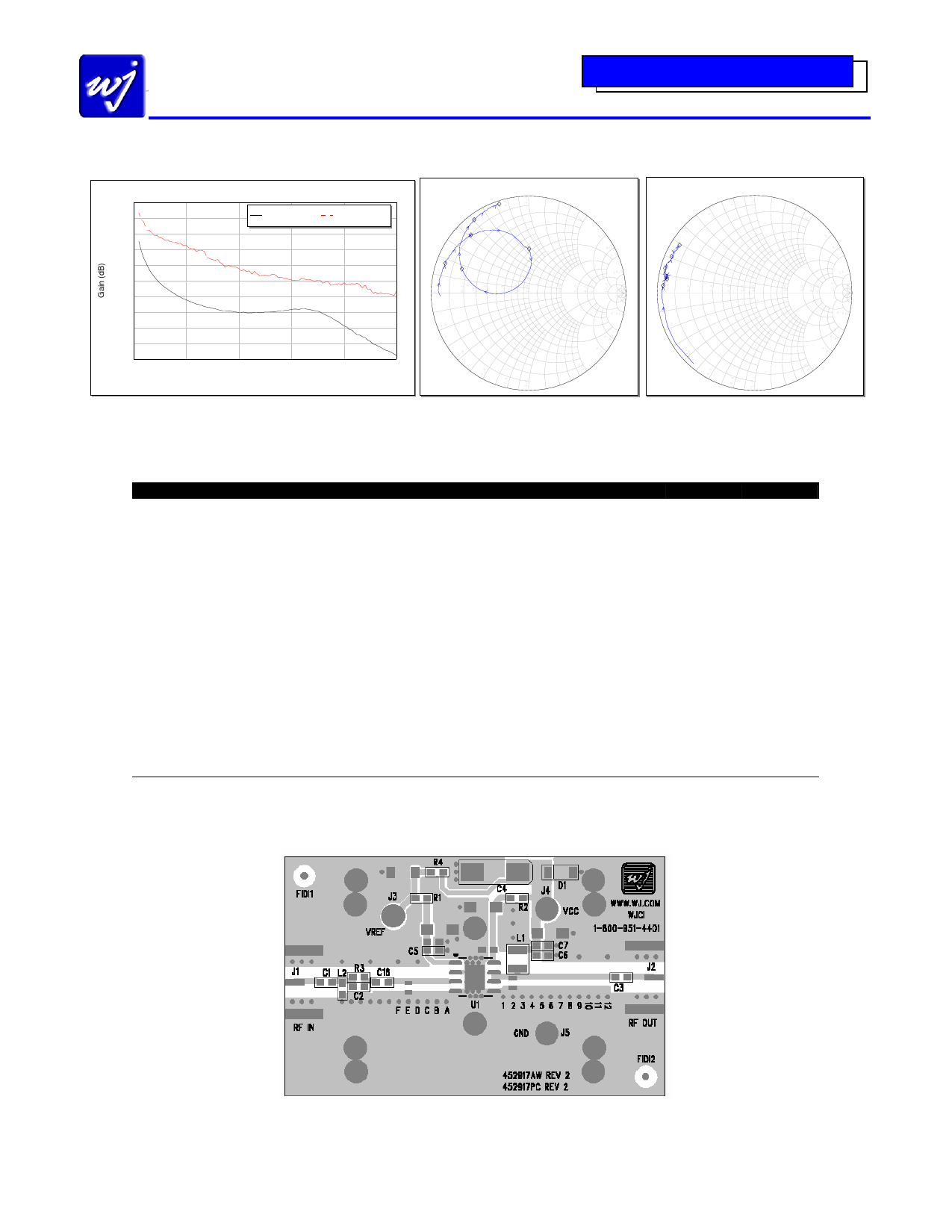
S-Parameters (VCC = +5 V, ICC = 800 mA, T = 25 °C, calibrated to device leads)
Gain / Maximum Stable Gain
40
35
DB(|S[2,1]|)
DB(GMax)
S11
Swp Max
3GHz
S22
30
3.0
25
4.0
5.0
20
10.0
15
10
5
0
-0.2
-0.2
-5
-10
-0.4
0
0.5
1
1.5
2
2.5
Frequency (GHz)
-0.4
Swp Min
0.05GHz
Notes:
The gain for the unmatched device in 50 ohm system is shown as the trace in black color. For a tuned circuit for a particular frequency,
it is expected that actual gain will be higher, up to the maximum stable gain. The maximum stable gain is shown in the dashed red line.
The impedance plots are shown from 50 – 3000 MHz, with markers placed at 0.5 – 3.0 GHz in 0.5 GHz increments.
Swp Max
3GHz
3.0
4.0
5.0
10.0
Swp Min
0.05GHz
S-Parameters (VCC = +5 V, ICC = 800 mA, T = 25 °C, unmatched 50 ohm system, calibrated to device leads)
Freq (MHz)
S11 (dB)
S11 (ang)
S21 (dB)
S21 (ang)
S12 (dB)
S12 (ang)
50
-0.86
-178.06
27.55
113.72
-45.75
30.91
100
-0.64
178.18
22.16
98.81
-45.46
12.80
200
-0.68
172.85
16.13
89.06
-42.65
6.09
400
-0.76
164.33
10.61
77.31
-43.96
4.69
600
-0.93
155.56
7.46
67.94
-41.17
6.70
800
-1.15
146.04
5.78
57.62
-41.65
-5.78
1000
-1.50
134.58
4.87
46.90
-40.36
-7.84
1200
-2.39
121.66
4.74
32.96
-40.22
-16.51
1400
-4.47
104.01
5.33
14.01
-38.97
-48.82
1600
-11.96
86.06
5.96
-17.55
-38.96
-86.32
1800
-8.66
-179.11
4.41
-56.78
-39.35
-144.53
2000
-2.76
159.91
0.53
-89.86
-43.55
145.94
2200
-1.21
142.90
-3.21
-107.99
-41.56
104.25
2400
-0.68
130.93
-7.27
-123.14
-42.46
73.64
2600
-0.43
121.91
-10.41
-134.93
-39.71
64.28
2800
-0.32
114.61
-13.28
-143.22
-40.99
58.20
3000
-0.29
108.16
-15.94
-149.93
-39.65
48.40
S22 (dB)
-0.38
-0.38
-0.48
-0.48
-0.61
-0.66
-0.71
-0.80
-0.76
-0.60
-0.52
-0.41
-0.54
-0.68
-0.73
-0.73
-0.79
Device S-parameters are available for download off of the website at: http://www.wj.com
S22 (ang)
-130.98
-157.30
-172.51
177.51
173.63
170.49
169.31
168.22
167.91
170.63
167.41
164.50
160.11
157.84
154.66
151.14
147.52
Application Circuit PC Board Layout
Circuit Board Material: .014” Getek, single layer, 1 oz copper, Microstrip line details: width = .026”, spacing = .026”
The silk screen markers ‘A’, ‘B’, ‘C’, etc. and ‘1’, ‘2’, ‘3’, etc. are used as placemarkers for the input and output tuning
shunt capacitors – C8 and C9. The markers and vias are spaced in .050” increments.
Specifications and information are subject to change without notice.
WJ Communications, Inc • Phone 1-800-WJ1-4401 • FAX: 408-577-6621 • e-mail: sales@wj.com • Web site: www.wj.com
Page 2 of 7 March 2006
Share Link: 