ADCMP607(Rev0) 查看數據表(PDF) - Analog Devices
零件编号
产品描述 (功能)
生产厂家
ADCMP607
(Rev.:Rev0)
(Rev.:Rev0)
Analog Devices

ADCMP607 Datasheet PDF : 16 Pages
| |||
ADCMP606/ADCMP607
TIMING INFORMATION
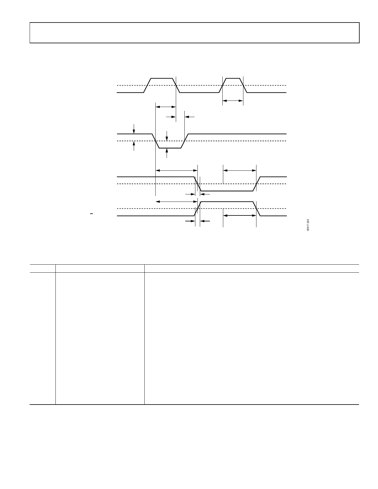
Figure 2 illustrates the ADCMP606/ADCMP607 latch timing relationships. Table 2 provides definitions of the terms shown in Figure 2.
LATCH ENABLE
tS
tPL
tH
DIFFERENTIAL
VIN
INPUT VOLTAGE
VOD
1.1V
VN ± VOS
Q OUTPUT
Q OUTPUT
tPDL
tPLOH
50%
tPDH
tF
50%
tR
Figure 2. System Timing Diagram
tPLOL
Table 2. Timing Descriptions
Symbol Timing
tF
Output fall time
tH
Minimum hold time
tPDH
Input to output high delay
tPDL
Input to output low delay
tPL
Minimum latch enable pulse width
tPLOH
Latch enable to output high delay
tPLOL
Latch enable to output low delay
tR
Output rise time
tS
Minimum setup time
VOD
Voltage overdrive
Description
Amount of time required to transition from a high to a low output as measured at the 20%
and 80% points.
Minimum time after the negative transition of the latch enable signal that the input signal
must remain unchanged to be acquired and held at the outputs.
Propagation delay measured from the time the input signal crosses the reference (± the
input offset voltage) to the 50% point of an output low-to-high transition.
Propagation delay measured from the time the input signal crosses the reference (± the
input offset voltage) to the 50% point of an output high-to-low transition.
Minimum time that the latch enable signal must be high to acquire an input signal change.
Propagation delay measured from the 50% point of the latch enable signal low-to-high
transition to the 50% point of an output low-to-high transition.
Propagation delay measured from the 50% point of the latch enable signal low-to-high
transition to the 50% point of an output high-to-low transition.
Amount of time required to transition from a low to a high output as measured at the 20%
and 80% points.
Minimum time before the negative transition of the latch enable signal occurs that an
input signal change must be present to be acquired and held at the outputs.
Difference between the input voltages VA and VB.
Rev. 0 | Page 5 of 16
Share Link: