SOMC14 查看數據表(PDF) - Vishay Semiconductors
零件编号
产品描述 (功能)
生产厂家
SOMC14
Vishay Semiconductors

SOMC14 Datasheet PDF : 5 Pages
| |||
www.vishay.com
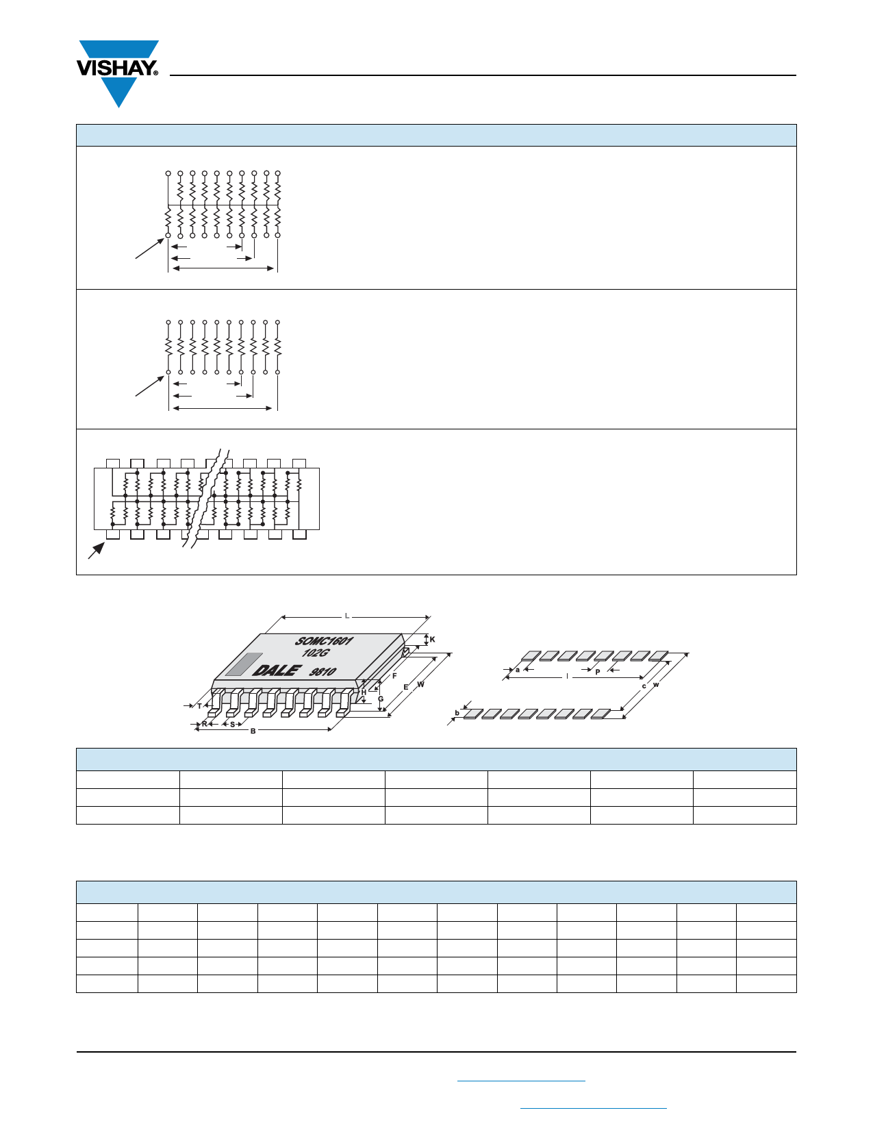
CIRCUIT APPLICATIONS
01 Schematic
Pin 1
03 Schematic
SOMC14
SOMC16
SOMC20
Pin 1
05 Schematic
SOMC14
SOMC16
SOMC20
R1 R1 R1 R1
R2
R2
R2
R1
R1
R1 R1
R2 R2
R2 R2
R1 R1 R1
R2 R2 R2
R1 R1 R1
R2 R2 R2 R2
Pin 1
SOMC14, SOMC16, SOMC20
DIMENSIONS
SOMC
Vishay Dale
13, 15, or 19 resistors with one pin common
The SOMCxx01 circuit provides a choice of 13, 15, or 19 nominally equal resistors, each
connected between a common lead (14, 16, or 20) and a discrete PC board pin.
Commonly used in the following applications:
• MOS/ROM pull-up/pull-down
• Open collector pull-up
• “Wired OR” pull-up
• Power driven pull-up
• TTL input pull-down
• Digital pulse squaring
• TTL unused gate pull-up
• High speed parallels pull-up
7, 8, or 10 isolated resistors
The SOMCxx03 circuit provides a choice of 7, 8, or 10 nominally equal resistors with each
resistor isolated from all others and wired directly across. Commonly used in the following
applications:
• “Wired OR” pull-up
• Power driven pull-up
• Powergate pull-up
• Line termination
• Long-line Impedance balancing
• LED current limiting
• ECL output pull-down
• TTL input pull-down
TTL dual-line terminator; pulse squaring, 12, 14, or 18 pairs of resistors
(R1 resistors are common to leads 14, 16, or 20)
(R2 resistors are common to leads 7, 8, or 10)
The SOMCxx05 circuit contains 12, 14, or 18 pairs of resistors. Each pair is connected
between ground and a common line. The junctions of these resistor pairs are connected
to the input leads.
The 05 circuits are designed for TTL dual-line termination and pulse squaring.
Pin 1
SOLDER PAD DIMENSIONS in millimeters
a
b
c
l
p
w
WAVE
0.64
1.91
5.34
9.53
1.27
9.15
REFLOW
0.64
1.91
5.34
9.53
1.27
9.15
Notes
• The dimension shown are for a 16 pin part. For parts with different pin numbers use the same pitch and add or subtract pads as required
• Maximum solder reflow temperature +255 °C
DIMENSIONS in millimeters
PIN NO#
L
W
B
E
F
G
H
K
R
S
T
14
9.91
7.62
7.62
6.20
5.59
2.16
2.03
0.914
0.457
1.27
1.14
16
11.18
7.62
8.89
6.20
5.59
2.16
2.03
0.914
0.457
1.27
1.14
20
13.72
7.62
11.43
6.20
5.59
2.16
2.03
0.914
0.457
1.27
1.14
Tol.
± 0.254 ± 0.381 ± 0.254 ± 0.381 ± 0.127 ± 0.127 ± 0.127
± 0.076 ± 0.254
MARKING INFORMATION
1 % parts have 4 digits while 2 % and 5 % parts have 3 digits.
Revision: 18-Apr-17
3
Document Number: 31508
For technical questions, contact: ff2aresistors@vishay.com
THIS DOCUMENT IS SUBJECT TO CHANGE WITHOUT NOTICE. THE PRODUCTS DESCRIBED HEREIN AND THIS DOCUMENT
ARE SUBJECT TO SPECIFIC DISCLAIMERS, SET FORTH AT www.vishay.com/doc?91000
Share Link: