FS6011-02 查看數據表(PDF) - AMI Semiconductor
零件编号
产品描述 (功能)
生产厂家
FS6011-02 Datasheet PDF : 15 Pages
| |||
)6
'LJLWDO $XGLR9LGHR &ORFN *HQHUDWRU ,&
X T
July 1998
Table 1: Pin Descriptions
Key: AI = Analog Input; AO = Analog Output; DI = Digital Input; DIU = Input with Internal Pull-Up; DID = Input with Internal Pull-Down; DIO = Digital Input/Output; DI-3 = Three-Level Digital Input,
DO = Digital Output; P = Power/Ground; # = Active Low pin
PIN
TYPE
NAME
DESCRIPTION
1
DI
SCLK
Serial Data Clock
2
DI
SDATA
Serial Data Input
3
DI
SLOAD
Serial Port Load
4
P
VSS
Ground
5
AI
XIN
VCXO Feedback
6
AO
XOUT
VCXO Drive
7
AI
XTUNE
VCXO Tune
8
P
VDD
Power Supply (+5V)
9
DID
PSEL1
PCLK Select MSB
10
DID
PSEL0
PCLK Select LSB
11
P
VSS
Ground
12
DO
PCLK
Processor Clock Output
13
DO
UCLK
Utility Clock Output
14
P
VDD
Power Supply (+5V)
15
DO
ACLK
Audio Clock Output
16
DO
CLK27
Reference Clock Output
3.0 Functional Block Description
3.1 Phase-Locked Loops
Each of the three on-chip PLLs in the FS6011 multiplies
the reference frequency to the desired frequency by a
ratio of integers. This frequency multiplication is exact.
3.2 Output Tristate Control
All four clock outputs of the FS6011 may be tristated to
facilitate circuit board testing. To place the outputs in
tristate mode, follow this sequence:
1. force XIN low (i.e. ground)
2. apply power to the device
3. wait until the internal power-on reset has deasserted
4. apply a negative-going transition to the PSEL0 pin
Outputs may be re-enabled by removing and reapplying
power to the FS6011. To re-enable outputs without re-
moving power, apply a rising edge transition to the XIN in
and follow it with a falling edge transition on the PSEL0
pin.
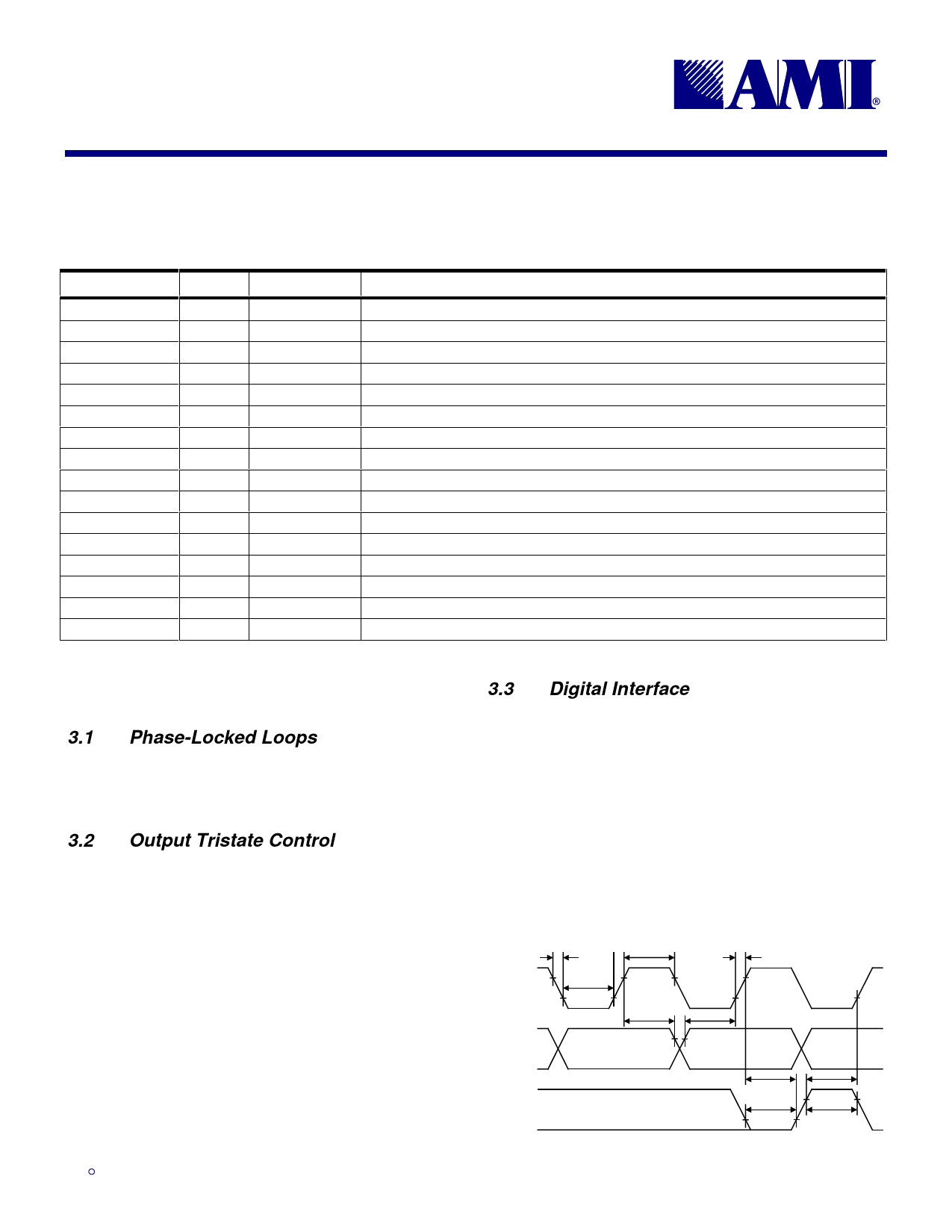
3.3 Digital Interface
Digital data is placed on the SDATA pin and clocked into
the FS6011 internal shift register (D[0] first) with a rising
edge on the SCLK pin. The shift register data is trans-
ferred to the FS6011 control registers with a rising edge
on the SLOAD pin. Fifteen bits must be shifted into the
internal registers before the parallel load can be per-
formed. In addition to the normal control functions per-
formed by D[13:0], there is one reserved bit, D[14], that
should be set to zero.
All control registers are initialized to zero on power-up.
Figure 3: Communications Protocol
SCLK
tF
tHI
tR
tLO
thd:DAT
tsu:DAT
SDATA
SLOAD
tsu:LD
tLO
thd:LD
tHI
2
,62
7.20.98
Share Link: 