54LVTH162373 查看數據表(PDF) - MAXWELL TECHNOLOGIES
零件编号
产品描述 (功能)
生产厂家
54LVTH162373 Datasheet PDF : 10 Pages
| |||
3.3V 16-Bit Transparent D-Type
54LVTH162373
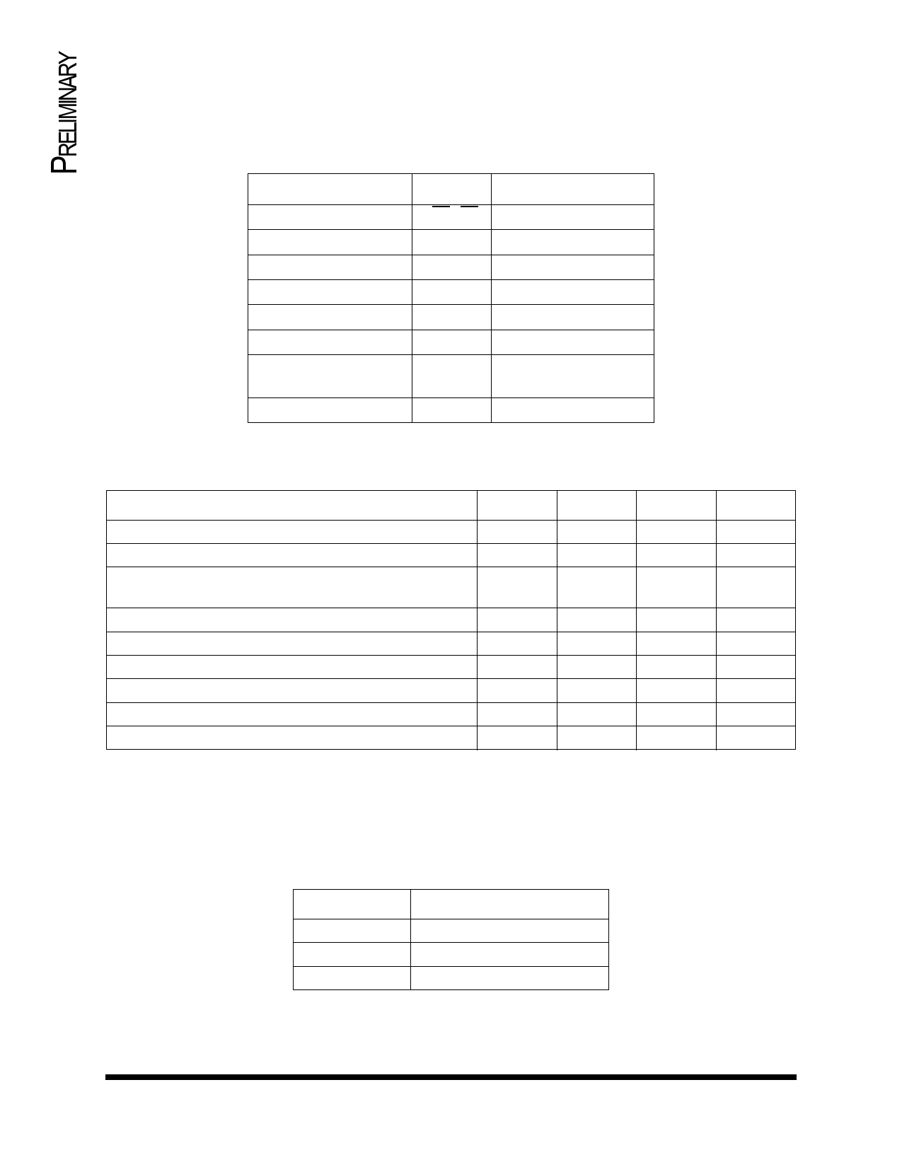
TABLE 1. PINOUT DESCRIPTION
PIN
SYMBOL
DESCRIPTION
1, 24
2, 3, 5, 6, 8, 9, 11, 12
4, 10, 15, 21, 28, 34, 39, 45
7, 31, 42
13, 14, 16, 17, 19, 20, 22, 23
25, 48
26, 27, 29, 30, 32, 31, 32,
33, 35, 36
37, 38, 40, 41, 43, 44, 46, 47
1OE-2OE
1Q1-1Q8
GND
VCC
2Q1-2Q8
2LE-1LE
2D8-2D1
1D8-1D1
Output Enable
Outputs
Ground
Power Supply
Outputs
Latch Enable
Inputs
Inputs
TABLE 2. 54LVTH162373 ABSOLUTE MAXIMUM RATINGS
PARAMETER
SYMBOL
MIN
MAX
UNIT
Supply voltage range
VCC
-0.5
4.6
V
Input voltage range 1
VI
-0.5
7
V
Voltage range applied to any output in the high state or power-off
VO
-0.5
7
V
state 1
Current into any output in the low state
Current into any output in the high state 2
Input clamp current (VI < 0)
Output clamp current (VO < O)
Maximum power dissipation at TA = 55°C 3
Storage temperature range
IO
--
30
mA
IO
--
30
mA
IIK
--
-50
mA
IOK
--
-50
mA
PD
--
0.85
mW
TS
-65
150
°C
1. The input and output negative-voltage ratings may be exceeded if the input and output clamp-current ratings are observed.
2. This current flows only when the output is in the high state and VO > VCC.
3. The maximum package power dissipation is calculated using a junction temperature of 150 °C and a board trace length of 750
mils.
TABLE 3. DELTA LIMITS
PARAMETER
VARIATION
ICC(OL)
ICC(OH)
ICC(OD)
±10% of specified value in Table 5
±10% of specified value in Table 5
±10% of specified value in Table 5
1000596
12.19.01 Rev 1
All data sheets are subject to change without notice 2
©2001 Maxwell Technologies
All rights reserved.
Share Link: 