74ACQ646CW 查看數據表(PDF) - Fairchild Semiconductor
零件编号
产品描述 (功能)
生产厂家
74ACQ646CW Datasheet PDF : 10 Pages
| |||
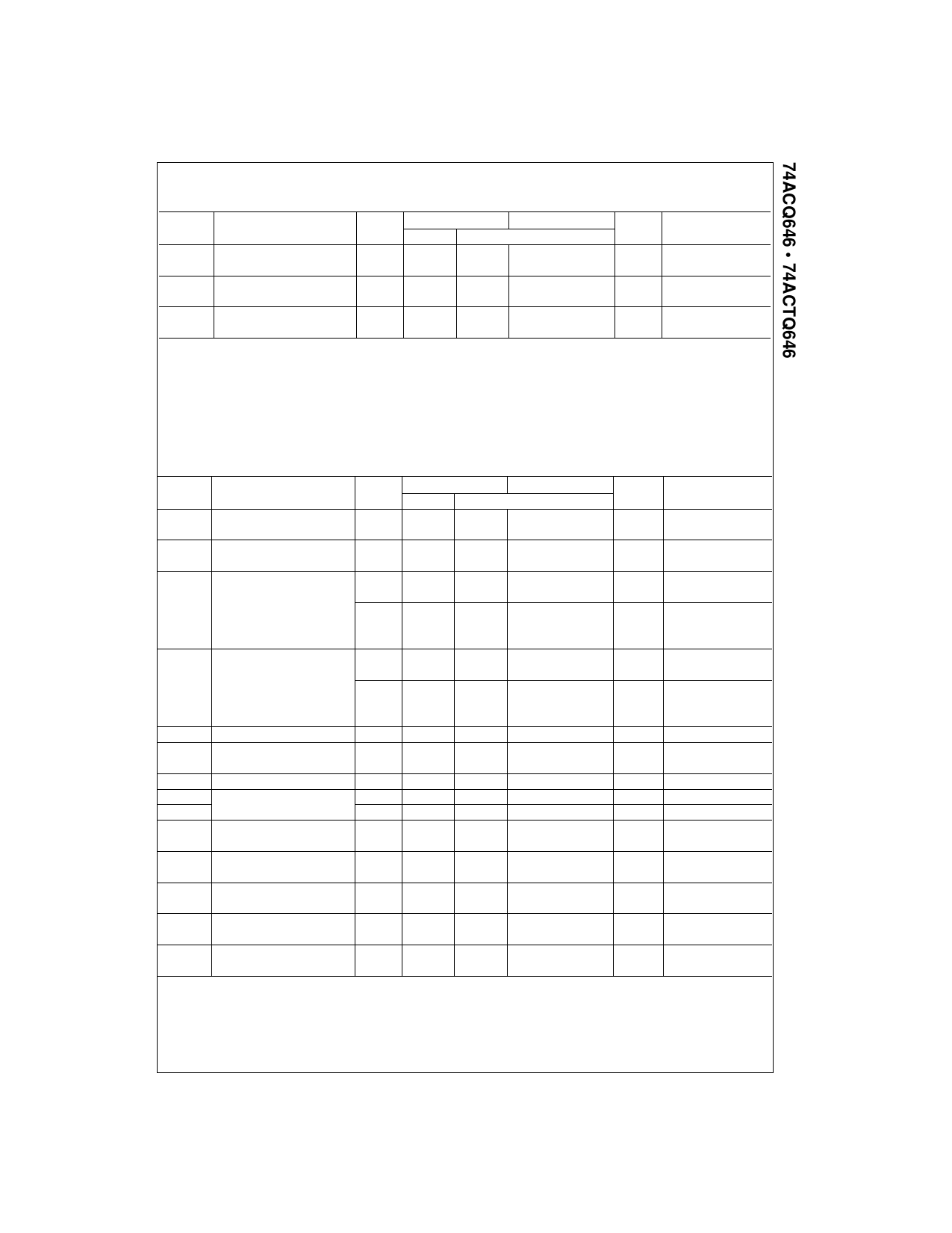
DC Electrical Characteristics for ACQ (Continued)
Symbol
Parameter
VCC
TA = +25°C
TA = −40°C to +85°C
Units
(V)
Typ
Guaranteed Limits
Conditions
VOLV
VIHD
Quiet Output
Minimum Dynamic VOL
Minimum HIGH Level
Dynamic Input Voltage
5.0
−0.6
−1.2
5.0
3.1
3.5
Figures 5, 6
V
(Note 6)(Note 7)
V (Note 6)(Note 8)
VILD
Maximum LOW Level
Dynamic Input Voltage
5.0
1.9
1.5
V (Note 6)(Note 8)
Note 3: Maximum of 8 outputs loaded; thresholds on input associated with output under test.
Note 4: Maximum test duration 2.0 ms, one output loaded at a time.
Note 5: IIN and ICC @ 3.0V are guaranteed to be less than or equal to the respective limit @ 5.5V VCC.
Note 6: Plastic DIP package.
Note 7: Max number of outputs defined as (n). Data inputs are driven 0V to 5V. One output @ GND.
Note 8: Max number of Data Inputs (n) switching. (n − 1) inputs switching 0V to 5V (ACQ). Input-under-test switching 5V to threshold (VILD),
0V to threshold (VIHD) f = 1 MHz.
DC Electrical Characteristics for ACTQ
Symbol
Parameter
VCC
TA = +25°C
TA = −40°C to +85°C
Units
(V)
Typ
Guaranteed Limits
Conditions
VIH
Minimum HIGH Level
Input Voltage
VIL
Maximum LOW Level
Input Voltage
VOH
Minimum HIGH Level
Output Voltage
4.5
1.5
2.0
2.0
5.5
1.5
2.0
2.0
4.5
1.5
0.8
0.8
5.5
1.5
0.8
0.8
4.5
4.49
4.4
4.4
5.5
5.49
5.4
5.4
V
VOUT = 0.1V
or VCC − 0.1V
V
VOUT = 0.1V
or VCC − 0.1V
V
IOUT = −50 µA
VOL
Maximum LOW Level
Output Voltage
4.5
3.86
3.76
5.5
4.86
4.76
4.5
0.001
0.1
0.1
5.5
0.001
0.1
0.1
VIN = VIL or VIH
V
IOH = −24 mA
IOH = −24 mA (Note 9)
V
IOUT = 50 µA
4.5
0.36
5.5
0.36
IIN
Maximum Input Leakage Current 5.5
±0.1
IOZT
Maximum I/O Leakage Current
5.5
±0.6
(An, Bn Inputs)
ICCT
Maximum ICC/Input
5.5
0.6
IOLD
Minimum Dynamic
5.5
IOHD
Output Current (Note 10)
5.5
ICC
Maximum Quiescent
5.5
8.0
Supply Current
0.44
0.44
±1.0
±6.0
1.5
75
−75
80.0
VIN = VIL or VIH
V
IOL = 24 mA
IOL = 24 mA (Note 9)
µA
VI = VCC, GND
µA
VI = VIL, VIH
VO = VCC, GND
mA VI = VCC − 2.1V
mA VOLD = 1.65V Max
mA VOHD = 3.85V Min
µA
VIN = VCC
or GND
VOLP
VOLV
VIHD
Quiet Output
Maximum Dynamic VOL
Quiet Output
Minimum Dynamic VOL
Minimum HIGH Level
Dynamic Input Voltage
5.0
1.1
1.5
5.0
−0.6
−1.2
5.0
1.7
2.0
Figures 5, 6
V
(Note 11)(Note 12)
Figures 5, 6
V
(Note 11)(Note 12)
V
(Note 11)(Note 13)
VILD
Maximum LOW Level
Dynamic Input Voltage
5.0
1.2
0.8
V
(Note 11)(Note 13)
Note 9: All outputs loaded; thresholds on input associated with output under test.
Note 10: Maximum test duration 2.0 ms, one output loaded at a time.
Note 11: Plastic DIP Package.
Note 12: Max number of outputs defined as (n). Data inputs are driven 0V to 3V. One output @ GND.
Note 13: Max number of data inputs (n) switching. (n − 1) inputs switching 0V to 3V (ACTQ). Input-under-test switching: 3V to threshold (VILD),
0V to threshold (VIHD), f = 1 MHz.
5
www.fairchildsemi.com
Share Link: 