ACASA1100A2200P5AT 查看數據表(PDF) - Vishay Semiconductors
零件编号
产品描述 (功能)
生产厂家
ACASA1100A2200P5AT Datasheet PDF : 6 Pages
| |||
ACAS 0612 AT - Precision Automotive
Vishay Beyschlag Automotive Precision Thin Film Chip Resistor Array
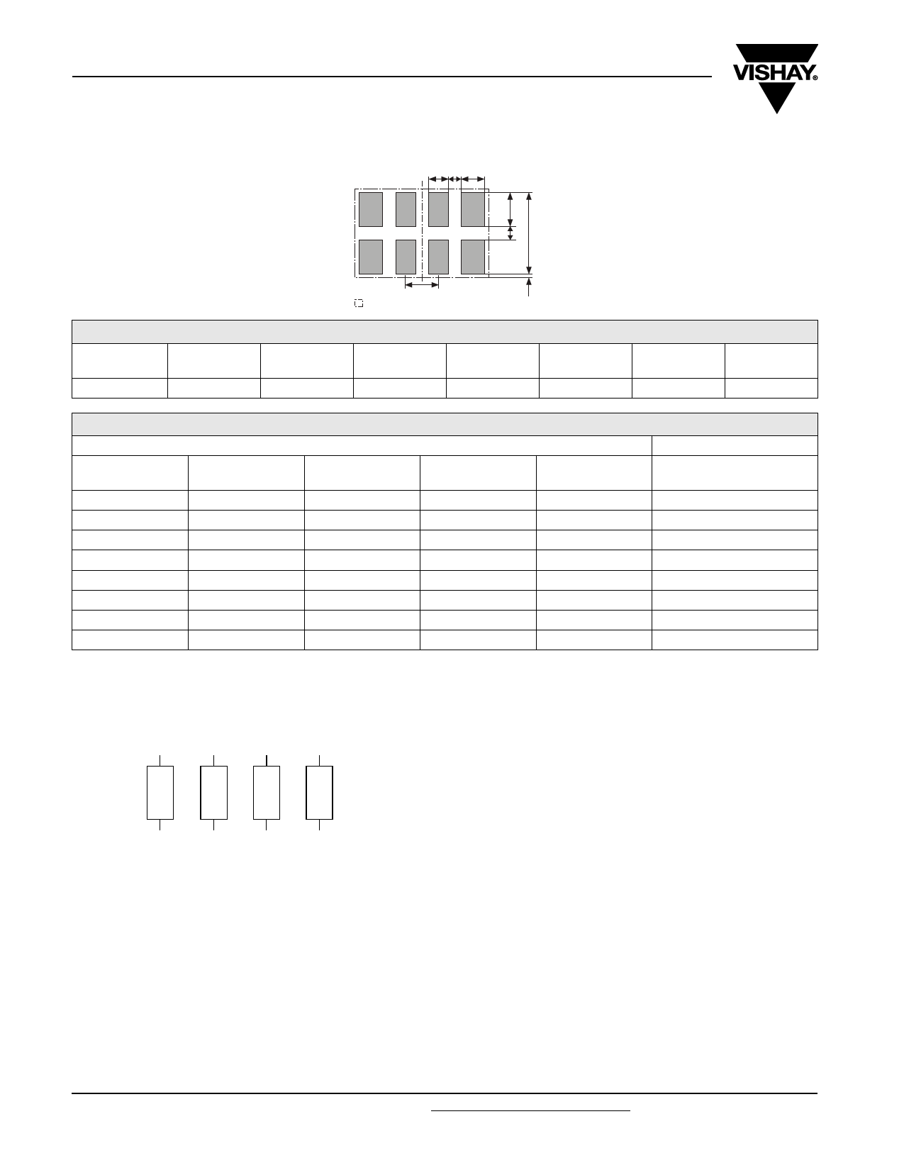
PATTERN STYLES FOR CHIP RESISTOR ARRAYS
UI X
Dimensions in mm
Y
G
Z
P
0.1
limits for solder resistance
RECOMMENDED SOLDER PAD DIMENSIONS FOR CHIP RESISTOR ARRAYS
TYPE
G
(mm)
Y
(mm)
X
(mm)
U
(mm)
Z
(mm)
I
(mm)
ACAS 0612 AT
0.8
1.15
0.64
0.44
3.1
0.36
P
(mm)
0.8
TEMPERATURE COEFFICIENT AND RESISTANCE RANGE
DESCRIPTION
RESISTANCE VALUE
ACCURACY
GRADE
ABSOLUTE TCR TCR TRACKING (1)
ABSOLUTE
TOLERANCE
TOLERANCE
MATCHING (1)
ACAS 0612 AT
A
± 25 ppm/K
10 ppm/K
± 0.25 %
0.1 %
47 Ω to 150 kΩ
B
± 25 ppm/K
10 ppm/K
± 0.5 %
0.25 %
47 Ω to 150 kΩ
E
± 25 ppm/K
15 ppm/K
± 0.25 %
0.1 %
47 Ω to 150 kΩ
F
± 25 ppm/K
15 ppm/K
± 0.5 %
0.25 %
47 Ω to 150 kΩ
J
± 25 ppm/K
25 ppm/K
± 0.25 %
0.1 %
47 Ω to 150 kΩ
K
± 25 ppm/K
25 ppm/K
± 0.5 %
0.25 %
47 Ω to 150 kΩ
N
± 50 ppm/K
25 ppm/K
± 0.5 %
0.5 %
47 Ω to 150 kΩ
P
± 50 ppm/K
50 ppm/K
± 0.5 %
0.5 %
47 Ω to 150 kΩ
Note
(1) In applications with defined resistance ratios like voltage dividers or feedback circuits, an array with a defined tracking of e.g. 10 ppm/K is
required to replace discrete resistors with a temperature coefficient of ± 5 ppm/K. Furthermore, in order to achieve the same tolerance of
± 0.05 % of individual resistors, an array requires a matching of 0.1 %.
APPLICATION INFORMATION
R1
R2
R3
R4
Circuit Type 03
DESCRIPTION
The production of the components is strictly controlled and
follows an extensive set of instructions established for
reproducibility. A homogeneous film of metal alloy is
deposited on a high grade (96 % Al2O3) ceramic substrate
and conditioned to achieve the desired temperature
coefficient. Specially designed inner contacts are realised on
both sides. A special laser is used to achieve the target value
by smoothly cutting a meander groove in the resistive layer
without damaging the ceramics.
The resistor elements are covered by a protective coating
designed for electrical, mechanical and climatic protection.
The terminations receive a final pure tin on nickel plating.
The result of the determined production is verified by an
extensive testing procedure and optical inspection
performed on 100 % of the individual chip resistors. Only
accepted products are laid directly into the paper tape in
accordance with IEC 60286-3*.
ASSEMBLY
The resistors are suitable for processing on automatic
SMD assembly systems. They are suitable for automatic
soldering using reflow or vapour phase as shown in
IEC 61760-1*. The encapsulation is resistant to all cleaning
solvents commonly used in the electronics industry,
including alcohols, esters and aqueous solutions.
The suitability of conformal coatings, if applied, shall be
qualified by appropriate means to ensure the long-term
stability of the whole system. The resistors are RoHS
compliant; the pure tin plating provides compatibility with
lead (Pb)-free and lead-containing soldering processes. The
permitted storage time is 20 years, whereas the solderability
is specified for 2 years after production or requalification. The
immunity of the plating against tin whisker growth has been
proven under extensive testing.
www.vishay.com
278
For technical questions, contact: filmresistors.thinfilmarray@vishay.com
Document Number: 28770
Revision: 11-Sep-08
Share Link: 