APU3037 查看數據表(PDF) - Advanced Power Electronics Corp
零件编号
产品描述 (功能)
生产厂家
APU3037 Datasheet PDF : 18 Pages
| |||
APU3037 / APU3037A
6) Place second pole at the ESR zero.
FP2 = FESR
R8 =
1
2p 3 C10 3 FP2
1
Check if R8 > gm
If R8 is too small, increase R7 and start from step 2.
7) Place second zero around the resonant frequency.
FZ2 = FLC
R6 =
2p 3
1
C10 3 FZ2
-
R8
8) Use equation (1) to calculate R5.
R5 =
VREF
VOUT - VREF
3 R6
Start to place the power components, make all the con-
nection in the top layer with wide, copper filled areas.
The inductor, output capacitor and the MOSFET should
be close to each other as possible. This helps to reduce
the EMI radiated by the power traces due to the high
switching currents through them. Place input capacitor
directly to the drain of the high-side MOSFET, to reduce
the ESR replace the single input capacitor with two par-
allel units. The feedback part of the system should be
kept away from the inductor and other noise sources,
and be placed close to the IC. In multilayer PCB use
one layer as power ground plane and have a control cir-
cuit ground (analog ground), to which all signals are ref-
erenced. The goal is to localize the high current path to
a separate loop that does not interfere with the more
sensitive analog control function. These two grounds
must be connected together on the PC board layout at a
single point.
These design rules will give a crossover frequency ap-
proximately one-tenth of the switching frequency. The
higher the band width, the potentially faster the load tran-
sient speed. The gain margin will be large enough to
provide high DC-regulation accuracy (typically -5dB to -
12dB). The phase margin should be greater than 458 for
overall stability.
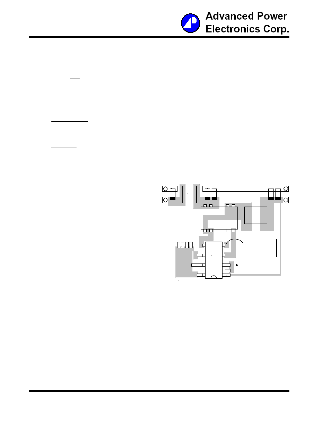
Figure 8 shows a suggested layout for the critical com-
ponents, based on the schematic on page 14.
PGnd
C1
L1
Vin
C2A, B
PGnd
PGnd
C7A, B
Vout
87
65
IC Quiescent Power Dissipation
Power dissipation for IC controller is a function of ap-
plied voltage, gate driver loads and switching frequency.
The IC's maximum power dissipation occurs when the
IC operating with single 12V supply voltage (Vcc=12V
and Vc≅24V) at 400KHz switching frequency and maxi-
mum gate loads.
Figures 9 and 10 show voltage vs. current, when the
gate drivers loaded with 470pF, 1150pF and 1540pF ca-
pacitors. The IC's power dissipation results to an exces-
sive temperature rise. This should be considered when
using APU3037A for such application.
Layout Consideration
The layout is very important when designing high fre-
quency switching converters. Layout will affect noise
pickup and can cause a good design to perform with
less than expected results.
L2
Q1
12
34
D DD C
3 21 5
5
4
C4 6 U1 3
PGnd APU3037
R4 C9 7
2 C3
C8 8
Analog Gnd
R5
1 R6
Single Point
Analog Gnd
Connect to
Power Ground plane
Analog Gnd
Figure 8 - Suggested layout.
(Topside shown only)
10/18
Share Link: 