29C010A 查看數據表(PDF) - Atmel Corporation
零件编号
产品描述 (功能)
生产厂家
29C010A Datasheet PDF : 18 Pages
| |||
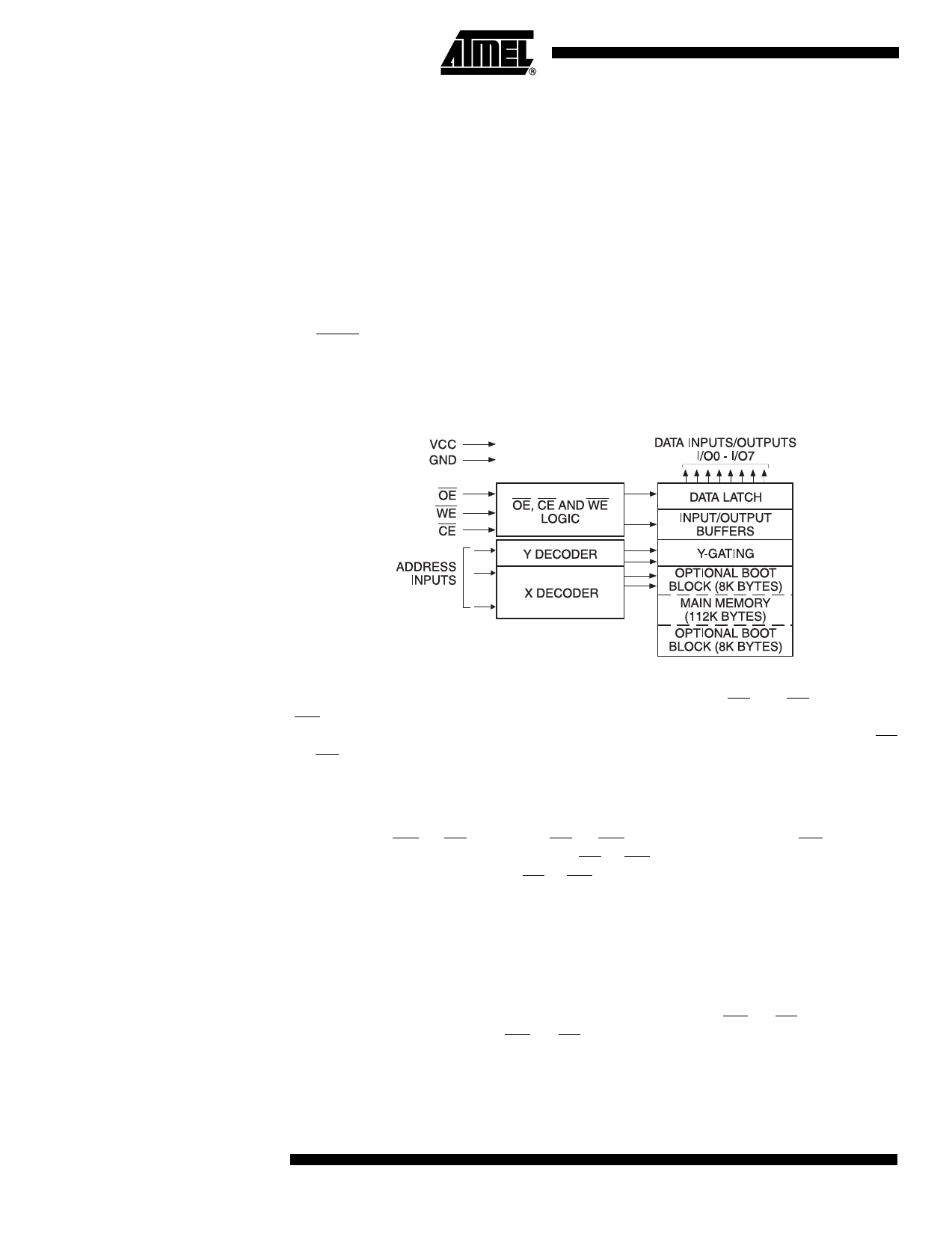
Block Diagram
less than 100 µA. The device endurance is such that any sector can typically be written
to in excess of 10,000 times.
To allow for simple in-system reprogrammability, the AT29C010A does not require high
input voltages for programming. Five-volt-only commands determine the operation of
the device. Reading data out of the device is similar to reading from an EPROM. Repro-
gramming the AT29C010A is performed on a sector basis; 128 bytes of data are loaded
into the device and then simultaneously programmed.
During a reprogram cycle, the address locations and 128 bytes of data are internally
latched, freeing the address and data bus for other operations. Following the initiation of
a program cycle, the device will automatically erase the sector and then program the
latched data using an internal control timer. The end of a program cycle can be detected
by DATA polling of I/O7. Once the end of a program cycle has been detected, a new
access for a read or program can begin.
Device Operation
READ: The AT29C010A is accessed like an EPROM. When CE and OE are low and
WE is high, the data stored at the memory location determined by the address pins is
asserted on the outputs. The outputs are put in the high impedance state whenever CE
or OE is high. This dual-line control gives designers flexibility in preventing bus
contention.
BYTE LOAD: Byte loads are used to enter the 128 bytes of a sector to be programmed
or the software codes for data protection. A byte load is performed by applying a low
pulse on the WE or CE input with CE or WE low (respectively) and OE high. The
address is latched on the falling edge of CE or WE, whichever occurs last. The data is
latched by the first rising edge of CE or WE.
PROGRAM: The device is reprogrammed on a sector basis. If a byte of data within a
sector is to be changed, data for the entire sector must be loaded into the device. The
data in any byte that is not loaded during the programming of its sector will be indetermi-
nate. Once the bytes of a sector are loaded into the device, they are simultaneously
programmed during the internal programming period. After the first data byte has been
loaded into the device, successive bytes are entered in the same manner. Each new
byte to be programmed must have its high to low transition on WE (or CE) within 150 ms
of the low to high transition of WE (or CE) of the preceding byte. If a high to low transi-
tion is not detected within 150 ms of the last low to high transition, the load period will
end and the internal programming period will start. A7 to A16 specify the sector address.
2 AT29C010A
0394E–FLASH–11/02
Share Link: 