B2526 查看數據表(PDF) - Unspecified
零件编号
产品描述 (功能)
生产厂家
B2526 Datasheet PDF : 7 Pages
| |||
B2526
ABSOLUTE MAXIMUM RATINGS
Supply Voltage…………………………………...6V
Fault Flag Voltage………………………………..6V
Fault Flag Current……………………………..50mA
Output Voltage……………………………………6V
Output Current……………………Internally Limited
Enable Input……………………………-0.3V to 12V
Storage Temperature………………-65°C to +150°C
Lead Temperature (Soldering 5 sec.)………….260°C
OPERATING RATING
Supply Voltage ..................................................+3V to +5.5V
Ambient Operating Temperature.................... -40°C to +85°C
Thermal Resistance
SOIC .................................................................. 120°C/W
DIP..................................................................... 130°C/W
ELECTRICAL CHARACTERISTICS at VIN = 5V, Ta=25°C, unless otherwise specified. (Note 1)
Parameters
Supply Current
Enable Input Threshold
Enable Input Current
Enable Input Capacitance
Switch Resistance
Output Turn-On Delay
Output Turn-On Rise Time
Output Turn-Off Delay
Output Turn-Off Fall Time
Output Leakage Current
Continuous Load Current
Short Circuit Current Limit
Current Limit Threshold
Over temperature Shutdown
Threshold
Error Flag Output Resistance
Error Flag Off Current
UVLO Threshold
Conditions
(Note1) Switch Off, OUT = Open
(Note1) Switch On, OUT = Open
Low to High Transition
High to Low Transition, (Note1)
VEN = 0V to 5.5V
VIN = 5V IOUT = 500mA, Each Switch
VIN = 3.3V IOUT = 500mA, Each Switch
RL = 10Ω
RL = 10Ω
RL = 10Ω
RL = 10Ω
Each output (output disabled)
Each output
Each output (enable into load), VOUT = 4.0V
Ramped Load applied to enable output, VOUT ≤ 4.0V
TJ Increasing
TJ Decreasing
VIN = 5.0V, IL = 10mA
VIN = 3.3V, IL = 10mA
VFLAG = 5V
VIN = Increasing
VIN = Decreasing
Typ
0.75
110
2.1
1.9
± 0.01
1
100
140
0.5
1
1
1
0.5
0.5
Min
0.8
-1
0.75
1.6
135
125
10
15
0.01
2.5
2.3
Max
5
160
2.4
1
140
180
20
20
10
1.25
2.2
1
Units
µA
V
µA
pF
mΩ
ms
ms
µs
µs
µA
A
A
A
°C
Ω
µA
V
General Note: Devices are ESD protected, however, handling precautions recommended.
Note 1: Off is ≤ 0.8V and is ≥ 2.4V for the B2526-1. Off is ≥ 2.4V and on is ≤ 0.8V for the B2526-2. The Enable input has approximately 200mV of hysteresis.
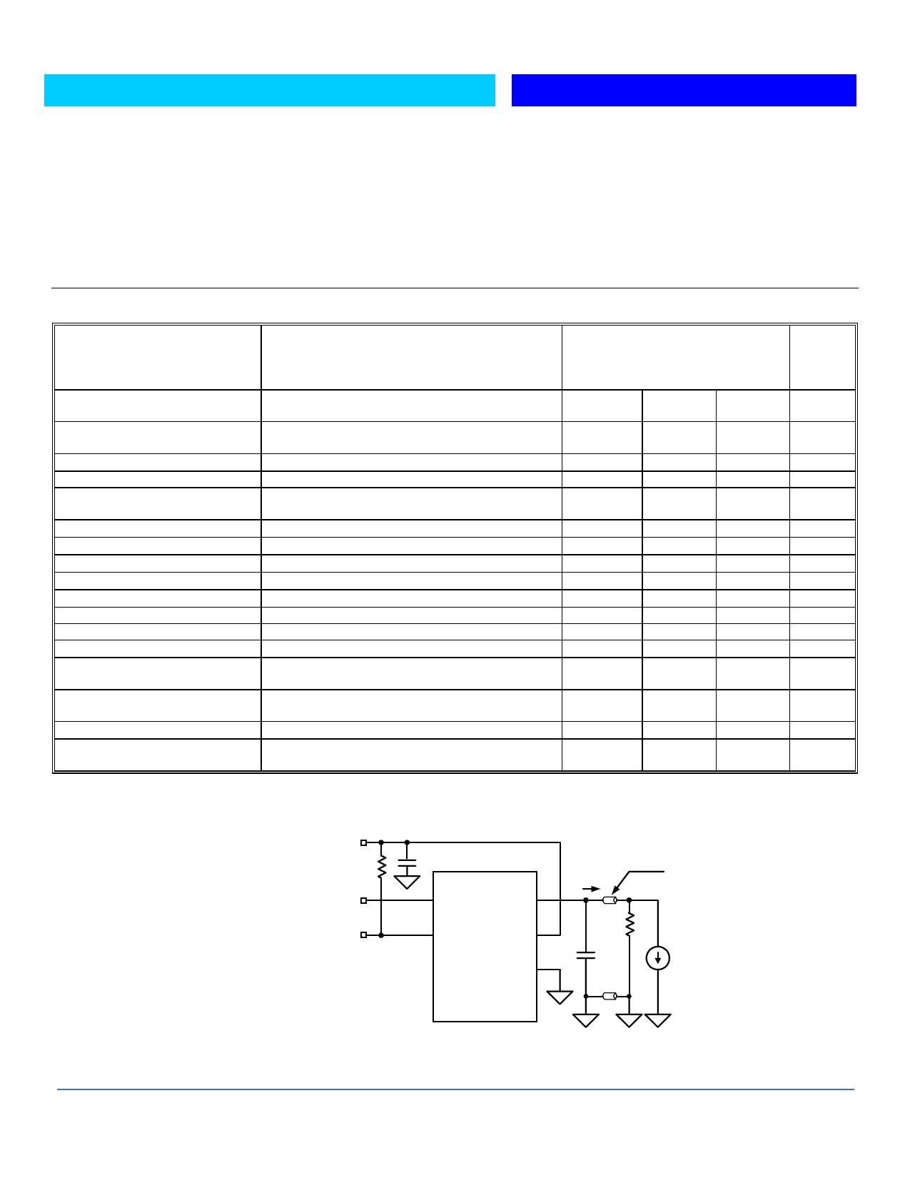
TEST CIRCUIT
(Only 1 Output Shown)
5V
10K
0.1µF
B2526
EN (A)
Out (A)
FLG (A)
IN
FLG (B)
EN (B)
GND
Out (B)
Ferrite
Bead
IOUT
RL
CL +
ILOAD
(for Current
Limit
Response)
Functional Characteristics Test Circuit
Bay Linear, Inc 2418Armstrong St., Livermore CA USA 94550 Tel: (925) 606-5950, Fax: (925) 940-9556
www.baylinear.com
Share Link: 