CAT33C804A 查看數據表(PDF) - Catalyst Semiconductor => Onsemi
零件编号
产品描述 (功能)
生产厂家
CAT33C804A Datasheet PDF : 14 Pages
| |||
CAT33C804A
Preliminary
PASSWORD PROTECTION
The CAT33C804A is a 4K-bit E2PROM that features a
password protection scheme to prevent unauthorized
access to the information stored in the device. It contains
an access code register which stores one to eight bytes
of access code along with the length of that access code.
Additionally, a memory pointer register stores the ad-
dress that partitions the memory into protected and
unprotected areas. As shipped from the factory, the
device is unprogrammed and unprotected. The length of
the access code is equal to zero and the memory pointer
register points to location zero. Every byte of the device
is fully accessible without an access code. Setting a
password and moving the memory pointer register to
cover all or part of the memory secures the device. Once
secured, the memory is divided into a read/write area
and a read-only area with the entry of a valid access
code. If no access code is entered, the memory is
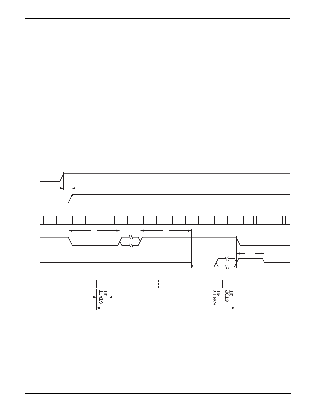
Figure 1. A.C. Timing
divided into a read-only area and a non-access area.
Figure 2 illlustrates this partitioning of the memory array.
WRITE PROTECTION
Another feature of the CAT33C804A is WRITE-protec-
tion without the use of an access code. If the memory
pointer register is set to cover all or part of the memory,
without setting the access code register, the device may
be divided into an area which allows full access, and an
area which allows READ-only access. To write into the
READ-only area, the user can override the memory
pointer register for every WRITE instruction or he can
simply move the address in the memory pointer register
to uncover this area, and then write into the memory.
This mechanism prevents inadvertent overwriting of
important data in the memory without the use of an
access code. Figure 3 illustrates this partitioning of the
memory array.
VCC
CS
tVCCS
CLK
DI
tD
START BIT
tD
STOP BIT
DO
HIGH-Z
DATA TIMING
MARK
SPACE
BIT TIME
104 µs
Note:
(1) If PE pin = 1.
D0 D1 D2 D3 D4 D5
(1)
D6 D7
CHARACTER TIME @ 9600 BAUD
tHZ
HIGH-Z
33C804 F03
Doc. No. 25044-00 2/98
4
Share Link: 