CH1817LM 查看數據表(PDF) - Unspecified
零件编号
产品描述 (功能)
生产厂家
CH1817LM Datasheet PDF : 7 Pages
| |||
Cermetek Microelectronics, Inc.
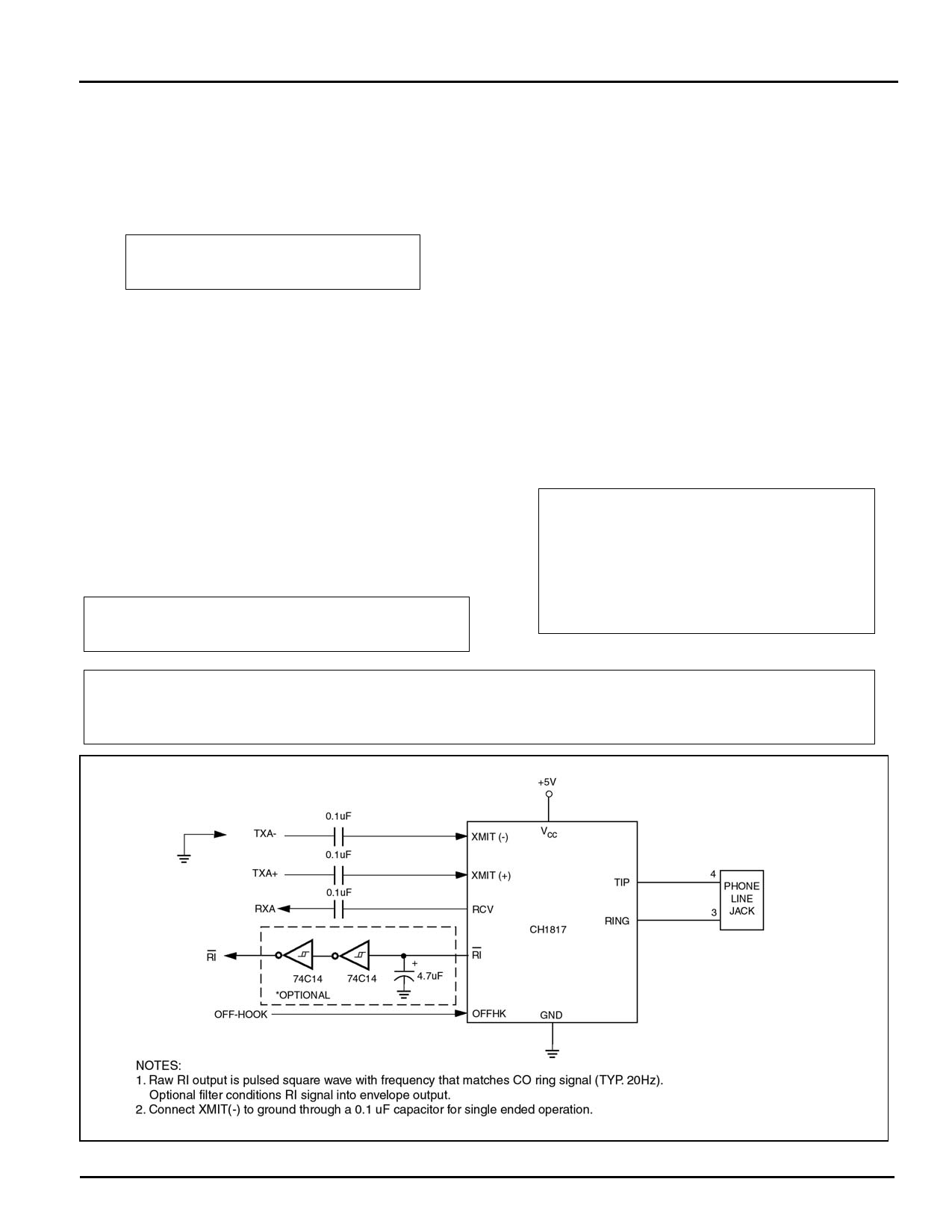
Hook Switch. The OFFHK input is used to control the
on-hook and off-hook status of the CH1817. When
OFFHK is low, the CH1817 is in the On-Hook State.
This indicates to the CO that the CH1817 is ready to
receive calls. When OFFHK is high, the CH1817
allows the CO supplied loop current to flow, indicating
either it is answering a call or preparing to place a call.
OFFHK
Input: Active High
Active Current: 4mA
CH1817 Family of Low Profile DAA Modules
TRANSMIT SIGNAL
The outgoing analog signal to be transmitted through
the phone line should be applied to the XMIT pin (with
respect to GND) and must be AC coupled as shown in
Figure 2. For the CH1817-D a XMIT (+) and XMIT (-)
pins provide a differential input. The CH1817-L
attenuates the transmit signal by 9.5dB, 0dB for the –D
option. Therefore, a transmit signal of 0dBm for the –L
option (-9.5 dB for –D) applied to XMIT will comply
with the FCC Part 68 requirement for data signals of –
9dBm across TIP and RING.
2-Wire To 4-Wire Hybrid Converter. This block has
two functions:
1. It applies the XMIT signal to the phone line.
2. It subtracts the desired signal from the total
outgoing signal on the phone line to derive the
RCV signal.
The accuracy of this derivation depends on how
closely the impedance of the phone line matches 600
Ohms. Generally, a small amount of the XMIT signal
will appear at RCV. The ratio of the applied XMIT
signal to the received XMIT signal is called Trans-
Hybrid Rejection, or Trans-Hybrid Loss. On a 600Ω
phone line, the CH1817 DAAs have very high trans-
hybrid rejection, typically 23 dB.
NOTE
The FCC requires that the DTMF tone not exceed
0dBm.
RECEIVE SIGNAL
The incoming analog signal appearing between TIP
and RING is presented at RCV with respect to GND
and must be AC coupled to the user equipment
receive input. The CH1817 does not gain the receive
signal. Receive signals can vary from a maximum
strength of –9dBm to below –50dBm.
RCV
Gain: 0dB
Out impedance: 100Ω
Typical Output Signal:
-9dBm to –50dBm
2.5Vrms to 0.27mVrms
Signal referenced to GND
AC coupling required
Attenuation
Input Impedance
CH1817-D
0dBm
150KΩ
XMIT
CH1817-L
9.5dBm
150KΩ
CH1817-DM
6.5dBm
150KΩ
CH1817-LM
6.5dBm
150KΩ
Figure 2. Typical CH1817 Application.
2002 Cermetek Microelectronics, Inc.
Page 2
Document No. 607-0007 Revision B (01/02)
Share Link: 