CY7C1311BV18(2004) 查看數據表(PDF) - Cypress Semiconductor
零件编号
产品描述 (功能)
生产厂家
CY7C1311BV18 Datasheet PDF : 23 Pages
| |||
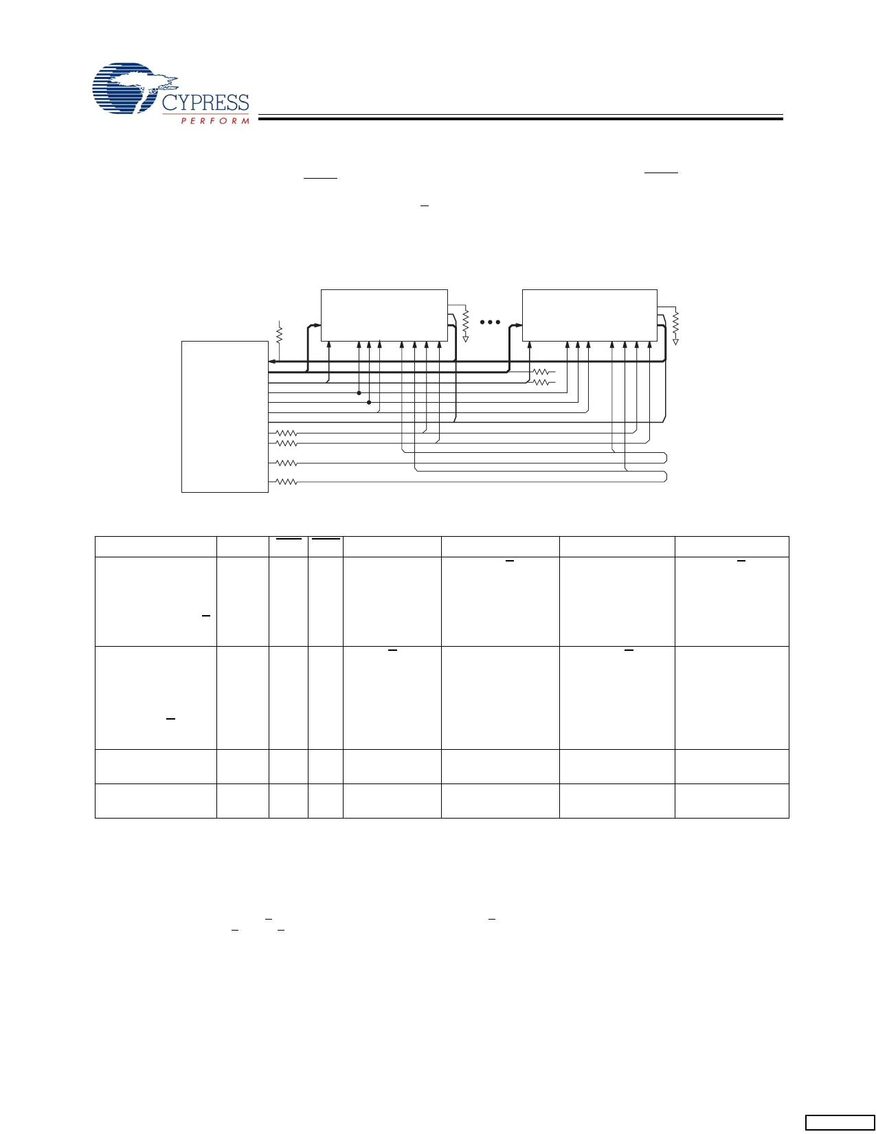
Application Example[1]
PRELIMINARY
CY7C1311BV18
CY7C1911BV18
CY7C1313BV18
CY7C1315BV18
SRAM #1
R = 250ohms
ZQ
Vt
RW B
CQ/CQ#
D
PPW
SS S
Q
R
A
# # # C C# K K#
DATA IN
DATA OUT
Address
RPS#
BUS
WPS#
MASTER
BWS#
(CPU CLKIN/CLKIN#
or
Source K
ASIC) Source K#
Delayed K
Delayed K#
R R = 50ohms Vt = Vddq/2
SRAM #4
ZQ R = 250ohms
RW B
CQ/CQ#
D
PPW
SS S
Q
A
## #
C C# K K#
Vt
Vt
R
Truth Table[2, 3, 4, 5, 6, 7]
Operation
K
Write Cycle:
L-H
Load address on the rising
edge of K; input write data on
two consecutive K and K
rising edges.
Read Cycle:
L-H
Load address on the rising
edge of K; wait one and a
half cycle; read data on two
consecutive C and C rising
edges.
NOP: No Operation
L-H
Standby: Clock Stopped Stopped
RPS
H[8]
WPS
DQ
L[9]
D(A) at
K(t+1) ↑
DQ
D(A + 1) at
K(t+1) ↑
DQ
DQ
D(A + 2) at K(t + D(A + 3) at
2) ↑
K(t +2) ↑
L[9]
X
Q(A) at
C(t +1)↑
Q(A + 1) at
C(t + 2) ↑
Q(A + 2) at C(t Q(A + 3) at C(t
+ 2)↑
+ 3) ↑
H
H
D=X
D=X
D=X
D=X
Q = High-Z Q = High-Z Q = High-Z Q = High-Z
X
X
Previous State Previous State Previous State Previous State
Write Cycle Descriptions CY7C1311BV18 and CY7C1313BV18) [2, 10]
BWS0/NWS0 BWS1/NWS1 K K
Comments
L
L
L–H – During the Data portion of a Write sequence:
CY7C1311BV18 − both nibbles (D[7:0]) are written into the device,
CY7C1313BV18 − both bytes (D[17:0]) are written into the device.
L
L
– L-H During the Data portion of a Write sequence:
CY7C1311BV18 − both nibbles (D[7:0]) are written into the device,
CY7C1313BV18 − both bytes (D[17:0]) are written into the device.
Notes:
1. The above application shows four QDR-II being used.
2. X = “Don't Care,” H = Logic HIGH, L = Logic LOW, ↑ represents rising edge.
3. Device will power-up deselected and the outputs in a tri-state condition.
4. “A” represents address location latched by the devices when transaction was initiated. A + 1, A + 2, and A +3 represents the address sequence in the burst.
5. “t” represents the cycle at which a Read/write operation is started. t + 1, t + 2, and t + 3 are the first, second and third clock cycles respectively succeeding the
“t” clock cycle.
6. Data inputs are registered at K and K rising edges. Data outputs are delivered on C and C rising edges, except when in single clock mode.
7. It is recommended that K = K and C = C = HIGH when clock is stopped. This is not essential, but permits most rapid restart by overcoming transmission line
charging symmetrically.
8. If this signal was LOW to initiate the previous cycle, this signal becomes a “Don’t Care” for this operation.
9. This signal was HIGH on previous K clock rise. Initiating consecutive Read or Write operations on consecutive K clock rises is not permitted. The device will
ignore the second Read or Write request.
10. Assumes a Write cycle was initiated per the Write Port Cycle Description Truth Table. NWS0, NWS1, BWS0, BWS1, BWS2 and BWS3 can be altered on different
portions of a Write cycle, as long as the set-up and hold requirements are achieved.
Document Number: 38-05620 Rev. **
Page 9 of 23
Share Link: 