CY7C1311BV18 查看數據表(PDF) - Cypress Semiconductor
零件编号
产品描述 (功能)
生产厂家
CY7C1311BV18 Datasheet PDF : 28 Pages
| |||
CY7C1311BV18
CY7C1911BV18
CY7C1313BV18
CY7C1315BV18
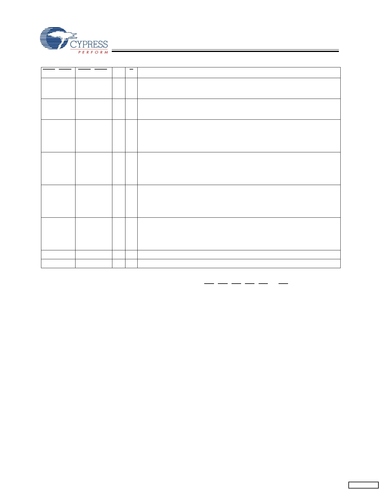
Write Cycle Descriptions (CY7C1311BV18 and CY7C1313BV18) [2, 10]
BWS0/NWS0 BWS1/NWS1 K K
Comments
L
L
L–H – During the Data portion of a Write sequence:
CY7C1311BV18 − both nibbles (D[7:0]) are written into the device,
CY7C1313BV18 − both bytes (D[17:0]) are written into the device.
L
L
– L-H During the Data portion of a Write sequence:
CY7C1311BV18 − both nibbles (D[7:0]) are written into the device,
CY7C1313BV18 − both bytes (D[17:0]) are written into the device.
L
H
L–H – During the Data portion of a Write sequence :
CY7C1311BV18 − only the lower nibble (D[3:0]) is written into the device. D[7:4] will
remain unaltered,
CY7C1313BV18 − only the lower byte (D[8:0]) is written into the device. D[17:9] will
remain unaltered.
L
H
– L–H During the Data portion of a Write sequence :
CY7C1311BV18 − only the lower nibble (D[3:0]) is written into the device. D[7:4] will
remain unaltered,
CY7C1313BV18 − only the lower byte (D[8:0]) is written into the device. D[17:9] will
remain unaltered.
H
L
L–H – During the Data portion of a Write sequence :
CY7C1311BV18 − only the upper nibble (D[7:4]) is written into the device. D[3:0] will
remain unaltered,
CY7C1313BV18 − only the upper byte (D[17:9]) is written into the device. D[8:0] will
remain unaltered.
H
L
– L–H During the Data portion of a Write sequence :
CY7C1311BV18 − only the upper nibble (D[7:4]) is written into the device. D[3:0] will
remain unaltered,
CY7C1313BV18 − only the upper byte (D[17:9]) is written into the device. D[8:0] will
remain unaltered.
H
H
L–H – No data is written into the devices during this portion of a write operation.
H
H
– L–H No data is written into the devices during this portion of a write operation.
Note:
10. Assumes a Write cycle was initiated per the Write Port Cycle Description Truth Table. NWS0, NWS1, BWS0, BWS1, BWS2 and BWS3 can be altered on different
portions of a Write cycle, as long as the set-up and hold requirements are achieved.
Document Number: 38-05620 Rev. *C
Page 10 of 28
[+] Feedback
Share Link: 