CY7C1311BV18 查看數據表(PDF) - Cypress Semiconductor
零件编号
产品描述 (功能)
生产厂家
CY7C1311BV18 Datasheet PDF : 28 Pages
| |||
CY7C1311BV18
CY7C1911BV18
CY7C1313BV18
CY7C1315BV18
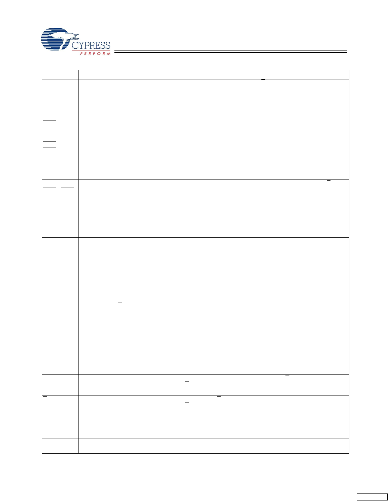
Pin Definitions
Pin Name
I/O
Pin Description
D[x:0]
WPS
NWS0,
NWS1,
Input-
Synchronous
Input-
Synchronous
Input-
Synchronous
Data input signals, sampled on the rising edge of K and K clocks during valid write opera-
tions.
CY7C1311BV18 − D[7:0]
CY7C1911BV18 − D[8:0]
CY7C1313BV18 − D[17:0]
CY7C1315BV18 − D[35:0]
Write Port Select, active LOW. Sampled on the rising edge of the K clock. When asserted active,
a Write operation is initiated. Deasserting will deselect the Write port. Deselecting the Write port
will cause D[x:0] to be ignored.
Nibble Write Select 0, 1 − active LOW.(CY7C1311BV18 Only) Sampled on the rising edge of
the K and K clocks during Write operations. Used to select which nibble is written into the device
NWS0 controls D[3:0] and NWS1 controls D[7:4].
All the Nibble Write Selects are sampled on the same edge as the data. Deselecting a Nibble
Write Select will cause the corresponding nibble of data to be ignored and not written into the
device.
BWS0, BWS1,
BWS2, BWS3
Input-
Synchronous
Byte Write Select 0, 1, 2, and 3 − active LOW. Sampled on the rising edge of the K and K clocks
during Write operations. Used to select which byte is written into the device during the current
portion of the Write operations. Bytes not written remain unaltered.
CY7C1911BV18 − BWS0 controls D[8:0]
CY7C1313BV18 − BWS0 controls D[8:0] and BWS1 controls D[17:9].
CY7C1315BV18 − BWS0 controls D[8:0], BWS1 controls D[17:9], BWS2 controls D[26:18] and
BWS3 controls D[35:27].
All the Byte Write Selects are sampled on the same edge as the data. Deselecting a Byte Write
Select will cause the corresponding byte of data to be ignored and not written into the device.
A
Input- Address Inputs. Sampled on the rising edge of the K clock during active Read and Write opera-
Synchronous tions. These address inputs are multiplexed for both Read and Write operations. Internally, the
device is organized as 2M x 8 (4 arrays each of 512K x 8) for CY7C1311BV18, 2M x 9 (4 arrays
each of 512K x 9) for CY7C1911BV18,1M x 18 (4 arrays each of 256K x 18) for CY7C1313BV18
and 512K x 36 (4 arrays each of 128K x 36) for CY7C1315BV18. Therefore, only 19 address
inputs are needed to access the entire memory array of CY7C1311BV18 and CY7C1911BV18,
18 address inputs for CY7C1313BV18 and 17 address inputs for CY7C1315BV18. These inputs
are ignored when the appropriate port is deselected.
Q[x:0]
RPS
Outputs-
Synchronous
Input-
Synchronous
Data Output signals. These pins drive out the requested data during a Read operation. Valid
data is driven out on the rising edge of both the C and C clocks during Read operations or K and
K. when in single clock mode. When the Read port is deselected, Q[x:0] are automatically
tri-stated.
CY7C1311BV18 − Q[7:0]
CY7C1911BV18 − Q[8:0]
CY7C1313BV18 − Q[17:0]
CY7C1315BV18 − Q[35:0]
Read Port Select, active LOW. Sampled on the rising edge of Positive Input Clock (K). When
active, a Read operation is initiated. Deasserting will cause the Read port to be deselected. When
deselected, the pending access is allowed to complete and the output drivers are automatically
tri-stated following the next rising edge of the C clock. Each Read access consists of a burst of
four sequential transfers.
C
Input- Positive Input Clock for Output Data. C is used in conjunction with C to clock out the Read
Clock data from the device. C and C can be used together to deskew the flight times of various devices
on the board back to the controller. See application example for further details.
C
Input- Negative Input Clock for Output Data. C is used in conjunction with C to clock out the Read
Clock data from the device. C and C can be used together to deskew the flight times of various devices
on the board back to the controller. See application example for further details.
K
Input- Positive Input Clock Input. The rising edge of K is used to capture synchronous inputs to the
Clock
device and to drive out data through Q[x:0] when in single clock mode. All accesses are initiated
on the rising edge of K.
K
Input- Negative Input Clock Input. K is used to capture synchronous inputs being presented to the
Clock
device and to drive out data through Q[x:0] when in single clock mode.
Document Number: 38-05620 Rev. *C
Page 6 of 28
[+] Feedback
Share Link: 