DMF-50174 وں¥çœ‹و•¸و“ڑè،¨ï¼ˆPDF) - Optrex Corporation
零ن»¶ç¼–هڈ·
ن؛§ه“پوڈڈè؟° (هٹں能)
ç”ںن؛§هژ‚ه®¶
DMF-50174 Datasheet PDF : 18 Pages
| |||
3.Optical Specifications
3.1.LCD Driving Voltage
Parameter
Symbol
Conditions
Min. Typ. Max. Units
Recommended
Ta= 0℃
ï¼چ
ï¼چ
27.1
V
LCD Driving Voltage
VCC-VADJ
Ta=25℃
21.7 23.3 24.9
V
Note 1
Ta=50℃
19.9
ï¼چ
ï¼چ
V
Note 1 : Voltage (Applied actual waveform to LCD Module) for the best contrast. The range of
minimum and maximum shows tolerance of the operating voltage. The specified contrast ratio and
response time are not guaranteed over the entire range.
3.2.Optical Characteristics
Ta=25℃, 1/240 Duty, 1/14 Bias, VD=23.3V (Note 4), خ¸= 0 ï¾ں, د†=ï¼چï¾ں
Parameter
Symbol
Conditions
Min. Typ. Max. Units
Contrast Ratio
Note 1
CR
خ¸= 0 ï¾ں, د†=ï¼چï¾ں
ï¼چ
4
ï¼چ
Viewing Angle
Shown in 3.3
Response Rise Note 2
TON
ï¼چ
ï¼چ
100
200
ms
Time Decay Note 3
TOFF
ï¼چ
ï¼چ
360
540
ms
Note 1 : Contrast ratio is definded as follows.
CR = LON / LOFF
LON : Luminance of the ON segments
LOFF : Luminance of the OFF segments
Note 2 : The time that the luminance level reaches 90% of the saturation level from 0% when ON
signal is applied.
Note 3 : The time that the luminance level reaches 10% of the saturation level from 100% when OFF
signal is applied.
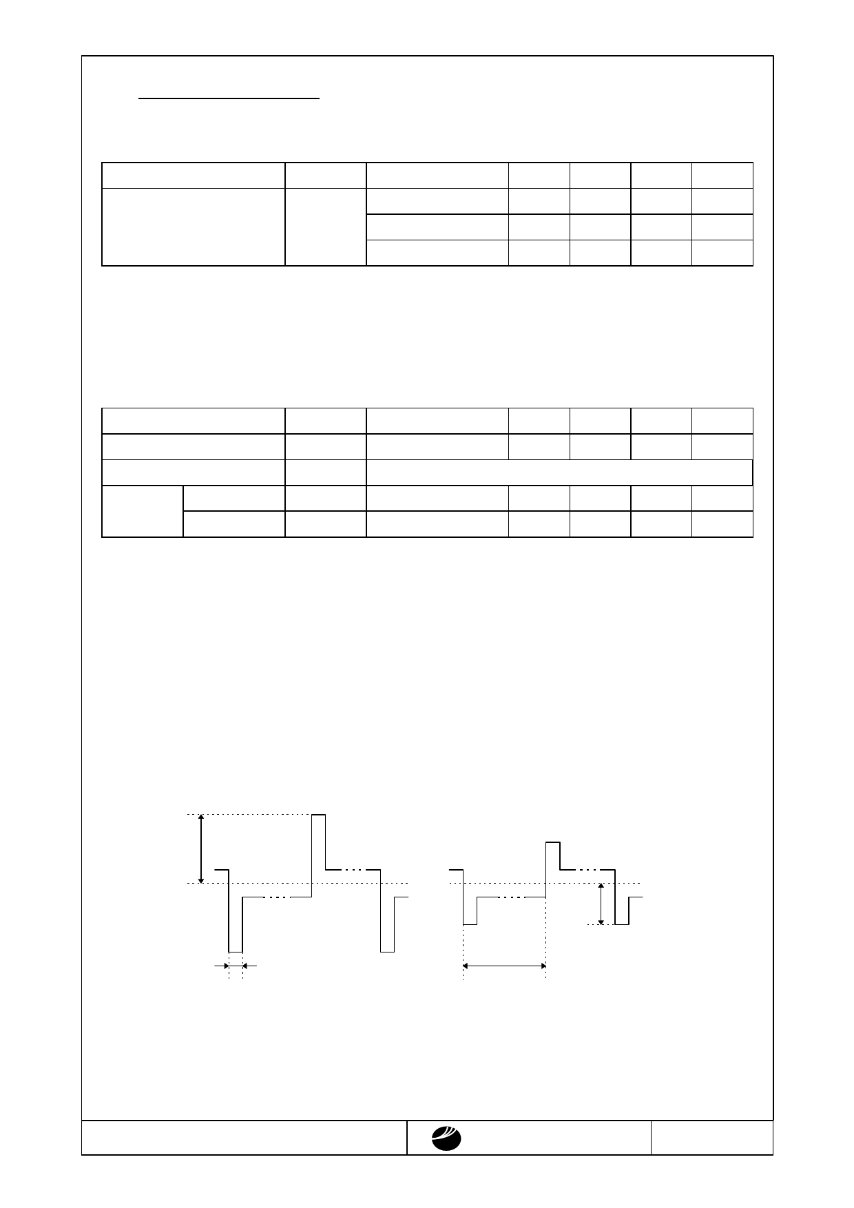
Note 4 : Definition of Driving Voltage VD
VD=VCC-VADJ-VBE
Assuming that the typical driving waveforms shown below are applied to the LCD Panel at
1/A Duty - 1/B Bias ( A : Duty Number, B : Bias Number ). Driving voltage VD is definded
as the voltage VO-P when the contrast ratio (CR=LON / LOFF) is at its maximum.
VO-P
1 / ( fFأ—A )
م€ˆON SIGNALم€‰
1 / fF
( B-2 )أ—VO-P / B
م€ˆOFF SIGNALم€‰
DMF-50174ZNB-FW (AT) No.2000-0166
OPTREX CORPORATION
OPTREX
Page 8/18
Share Link: 