E28F016SA-080 查看數據表(PDF) - Intel
零件编号
产品描述 (功能)
生产厂家
E28F016SA-080 Datasheet PDF : 55 Pages
| |||
28F016SA
E
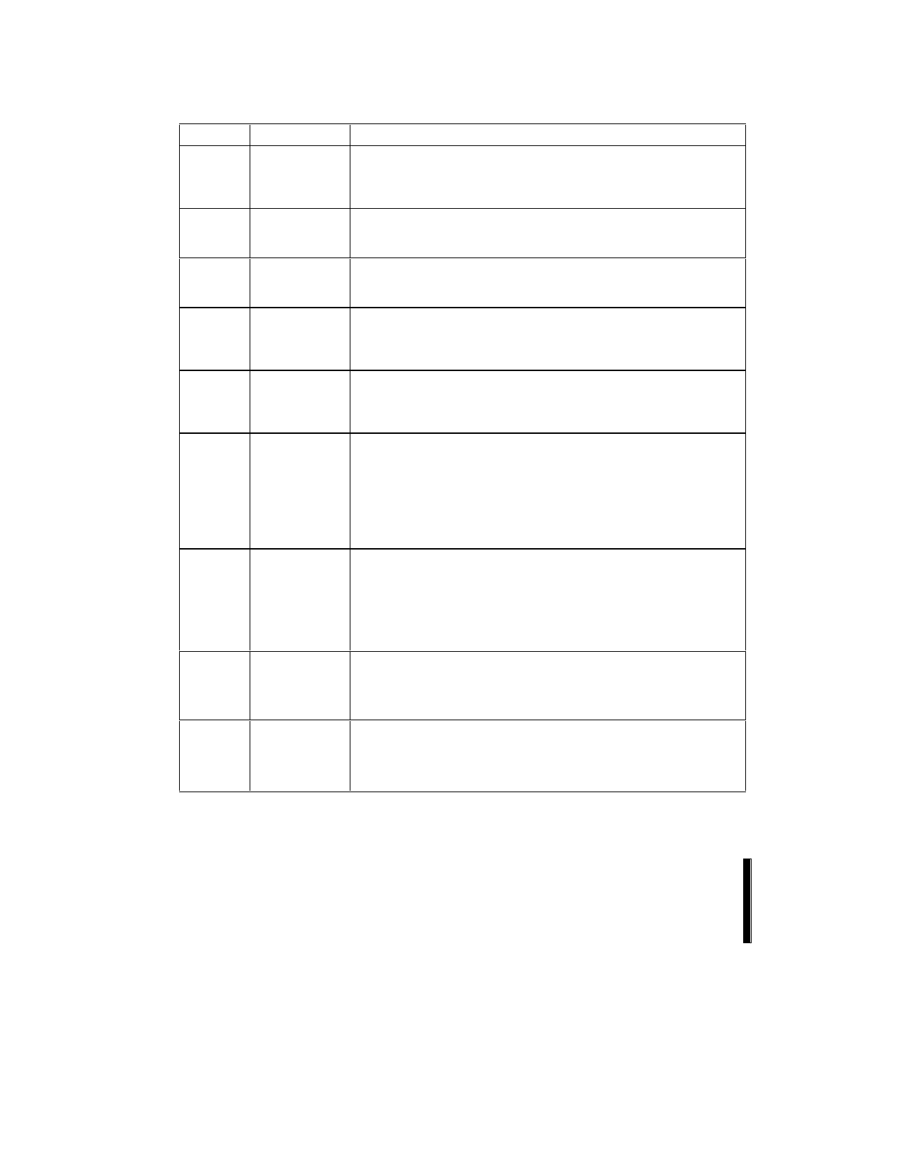
2.1 Lead Descriptions
Symbol
Type
Name and Function
A0
INPUT
BYTE-SELECT ADDRESS: Selects between high and low byte when the
device is in x8 mode. This address is latched in x8 data programs. Not
used in x16 mode (i.e., the A0 input buffer is turned off when BYTE# is
high).
A1–A15
INPUT
WORD-SELECT ADDRESSES: Select a word within one 64-Kbyte block.
A6–15 selects 1 of 1024 rows, and A1–5 selects 16 of 512 columns. These
addresses are latched during data programs.
A16–A20
INPUT
BLOCK-SELECT ADDRESSES: Select 1 of 32 erase blocks. These
addresses are latched during data programs, block erase and lock block
operations.
DQ0–DQ7
INPUT/OUTPUT
LOW-BYTE DATA BUS: Inputs data and commands during CUI write
cycles. Outputs array, buffer, identifier or status data in the appropriate
read mode. Floated when the chip is deselected or the outputs are
disabled.
DQ8–DQ15
INPUT/OUTPUT
HIGH-BYTE DATA BUS: Inputs data during x16 data program
operations. Outputs array, buffer or identifier data in the appropriate read
mode; not used for Status Register reads. Floated when the chip is
deselected or the outputs are disabled.
CE0#,CE1#
INPUT
CHIP ENABLE INPUTS: Activate the device’s control logic, input buffers,
decoders and sense amplifiers. With either CE0# or CE1# high, the device
is deselected and power consumption reduces to standby levels upon
completion of any current data program or block erase operations. Both
CE0#, CE1# must be low to select the device.
All timing specifications are the same for both signals. Device selection
occurs with the latter falling edge of CE0# or CE1#. The first rising edge of
CE0# or CE1# disables the device.
RP#
INPUT
RESET/POWER-DOWN: RP# low places the device in a deep power-
down state. All circuits that burn static power, even those circuits enabled
in standby mode, are turned off. When returning from deep power-down,
a recovery time is required to allow these circuits to power-up.
When RP# goes low, any current or pending WSM operation(s) are
terminated, and the device is reset. All Status Registers return to ready
(with all status flags cleared).
OE#
INPUT
OUTPUT ENABLE: Gates device data through the output buffers when
low. The outputs float to tri-state off when OE# is high.
NOTE:
CEx# overrides OE#, and OE# overrides WE#.
WE#
INPUT
WRITE ENABLE: Controls access to the CUI, Page Buffers, Data Queue
Registers and Address Queue Latches. WE# is active low, and latches
both address and data (command or array) on its rising edge.
Page Buffer addresses are latched on the falling edge of WE#.
8
Share Link: 