VSC8101QB 查看數據表(PDF) - Vitesse Semiconductor
零件编号
产品描述 (功能)
生产厂家
VSC8101QB Datasheet PDF : 14 Pages
| |||
VITESSE
VSC8101/8102
Preliminary Data Sheet
155.52 Mb/s Clock and
Data Recovery Units
Features
• Recovers Clock and Data at STS-3 (155.52 Mb/s)
Data Rate.
• No External Components Required.
• Available in One-channel (VSC8101) or
Eight-channel (VSC8102) Versions.
• Recovers Data from NRZ or NRZI Data Streams.
• No Output Clock Drift in Absence of Data
Transitions Once Lock is Acquired.
• ECL or Psuedo ECL (PECL) Differential Inputs
and Outputs.
• Maximum Power Dissipation:
VSC8101: 400mW,
VSC8102: 3W.
• Single 2V Power Supply
• Available in 28PLCC (VSC8101)
and 100PQFP (VSC8102)
Functional Description
The VSC8101 and VSC8102 are clock and data recovery units for STS-3 (155.52 Mb/s) applications. They
implement the complete clock and data recovery functions and require no external components. The one-chan-
nel device, VSC8101, accepts serial data in NRZ or NRZI format and re-times the data using a sampling clock
extracted from the input data stream. The recovered clock (RCLK+/-) and re-timed data (RDAT+/-) are pre-
sented at the serial output ports, aligned such that the falling edge of the recovered clock (RCLK+) coincides
with the center of the data eye (see figure 4). The VSC8102 is an octal version of the VSC8101. A single refer-
ence clock input (REFCK+/-) at the STS-3 data rate (155.52MHz) is required for either device. The data and
reference clock inputs, and the recovered data and clock outputs are differential ECL levels referenced to the
VCC supply. Only one supply, +2V or -2V, is required for operation.
Both the VSC8101 and VSC8102 employ a digital clock extraction technique, and do not contain a conven-
tional PLL. As a result, the spectrum of the jitter in the recovered clock and data is non-Gaussian. Peak-to-peak
jitter of RCLK+/- is ± 400 ps or less. The data input rate to the devices is required to be within ± 30 ppm from
the reference clock frequency. The devices have data input jitter accommodation up to 3.2ns, half the data
period. The VSC8101and VSC8102 also provide an input which control the loop bandwidth of the clock extrac-
tion function.
Tracking Frequency Bandwidth Control
The tracking of the recovered clock and data to the frequency variation of the input data stream can be
adjusted in the VSC8101 and VSC8102. In particular, the FILTER0 input controls the degree to which the inter-
nal clock can track the input data frequency. The effect is equivalent to controlling the loop bandwidth of a con-
ventional PLL-based clock recovery system. Equivalent bandwidths of 150 KHz and 10 KHz can be selected.
The FILTER0 input truth data is shown in the AC Characteristic Table.
Jitter Tolerance
The VSC8101 and VSC8102 are designed to meet the BellcoreGR-253-CORE, section 5.6.2.2.2 Jitter Tol-
erance specification.
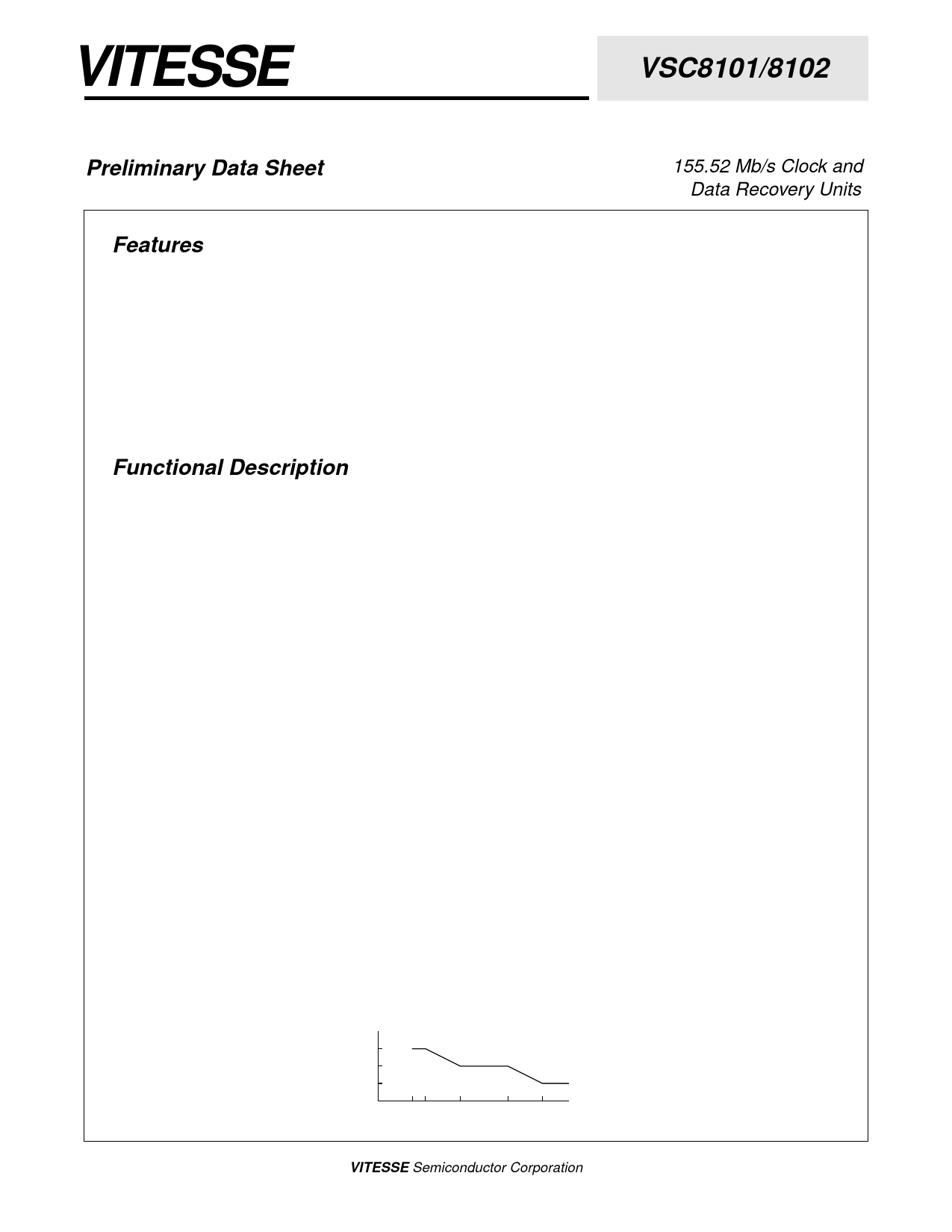
Figure 1: Jitter Tolerance Mask for STS-3
Jitter Amplitude
(UI p-p)
15
1.5
0.15
10 30
300
6.5K
65K
Frequency (Hz)
G52087-0 Rev. 1.3
® VITESSE Semiconductor Corporation
Page 1
Share Link: 