VSC8102 查看數據表(PDF) - Vitesse Semiconductor
零件编号
产品描述 (功能)
生产厂家
VSC8102 Datasheet PDF : 14 Pages
| |||
VSC8101/8102
VITESSE
155.52 Mb/s Clock and
Data Recovery Units
Preliminary Data Sheet
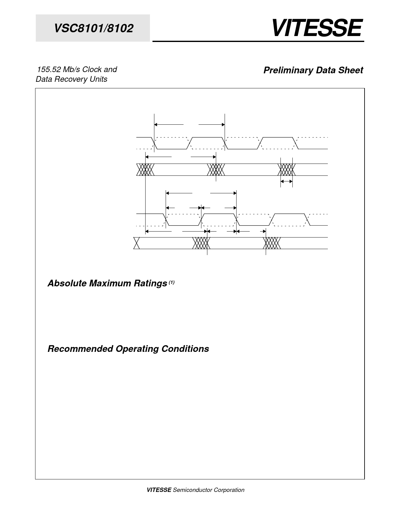
Figure 4: VSC8101/8102 AC Timing Waveform
(1)
REFCK+ / REFCK-
Reference Clock
SDAT+ / SDAT-
Input Data
tCLK
tDCYC
DATA IN (1)
DATA IN (2)
tRCYC
tDJA
(1)
RCLK+ / RCLK-
Recovered Clock
RDAT+ / RDAT-
Recovered Data
tRCL
tPD
VALID DATA (0)
tRCH
tDS
tDH
VALID DATA (1)
VALID DATA (2)
Note: (1) Solid line indicates the true sense and dotted line indicates the complementary sense of the signal.
Absolute Maximum Ratings (1)
Power Supply Voltage (VCC -VTT)..................................................................................................-0.5V to +3.0V
Input Voltage (VIN) ...................................................................................................... VCC -2.5V to VCC + 0.5V
Output Current, IOUT (DC, Output HI) .......................................................................................................-50mA
Case Temperature Under Bias, TC................................................................................................. -55° to +125°C
Storage Temperature (TSTG) ........................................................................................................-65°C to +135°C
Recommended Operating Conditions
The VSC8101 and VSC8102 can be powered by:
a) connecting VCC to +2V and VTT to GND, or
b) connecting VCC to GND and VTT to -2V.
Power Supply Voltage (VCC -VTT)........................................................................................................ 2.0V ± 5%
Operating Temperature Range(2) ........................................................................................................ 0° to +70°C
Notes:
(1) CAUTION: Stresses listed under “Absolute Maximum Ratings” may be applied to devices one at a time without causing pe
manent damage. Functionality at or above the values listed is not implied. Exposure to these values for extended periods
may affect device reliability.
(2) Lower limit is ambient temperature and upper limit is case temperature.
Page 4
® VITESSE Semiconductor Corporation
G52087-0 Rev. 1.3
Share Link: 