EDI88130CS17LM 查看數據表(PDF) - White Electronic Designs Corporation
零件编号
产品描述 (功能)
生产厂家
EDI88130CS17LM Datasheet PDF : 9 Pages
| |||
EDI88130CS
HI-RELIABILITY PRODUCT
128Kx8 Monolithic SRAM, SMD 5962-89598
FEATURES
s Access Times of 15*, 17, 20, 25, 35, 45, 55ns
s Battery Back-up Operation
• 2V Data Retention (EDI88130LPS)
s CS1, CS2 & OE Functions for Bus Control
s Inputs and Outputs Directly TTL Compatible
s Organized as 128Kx8
s Commercial, Industrial and Military Temperature Ranges
s Thru-hole and Surface Mount Packages JEDEC Pinout
• 32 pin Sidebrazed Ceramic DIP, 400 mil (Package 102)
• 32 pin Sidebrazed Ceramic DIP, 600 mil (Package 9)
• 32 lead Ceramic SOJ (Package 140)
• 32 pad Ceramic Quad LCC (Package 12)
• 32 pad Ceramic LCC (Package 141)
• 32 lead Ceramic Flatpack (Package 142)
s Single +5V (±10%) Supply Operation
The EDI88130CS is a high speed, high performance, 128Kx8 bits
monolithic Static RAM.
An additional chip enable line provides system memory security
during power down in non-battery backed up systems and memory
banking in high speed battery backed systems where large mul-
tiple pages of memory are required.
The EDI88130CS has eight bi-directional input-output lines to
provide simultaneous access to all bits in a word.
A low power version, EDI88130LPS, offers a 2V data retention
function for battery back-up applications.
Military product is available compliant to MIL-PRF-38535.
*15ns access time is advanced information, contact factory for availability.
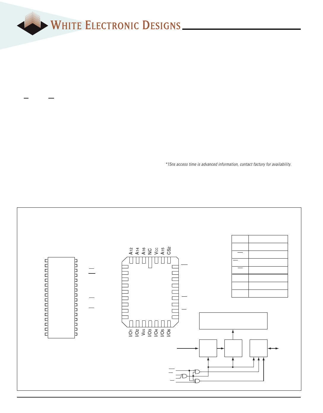
FIG. 1 PIN CONFIGURATION
32 DIP
32 SOJ
32 CLCC
32 FLATPACK
TOP VIEW
32 QUAD LCC
TOP VIEW
NC 1
A16 2
A14 3
A12 4
A7 5
A6 6
A5 7
A4 8
A3 9
A2 10
A1 11
AØ 12
I/OØ 13
I/O1 14
I/O2 15
VSS 16
32 VCC
31 A15
30 CS2
29 WE
28 A13
27 A8
26 A9
25 A11
24 OE
23 A10
22 CS1
21 I/O7
20 I/O6
19 I/O5
18 I/O4
17 I/O3
4 3 2 1 32 31 30
A7 5
29 WE
A6 6
28 A13
A5 7
27 A8
A4 8
26 A9
A3 9
25 A11
A2 10
24 OE
A1 11
23 A10
A0 12
22 CS1
I/O0 13
21 I/O7
14 15 16 17 18 19 20
AØ-16
PIN DESCRIPTION
I/O0-7 Data Inputs/Outputs
A0-16
Address Inputs
WE
Write Enable
CS1, CS2 Chip Selects
OE
Output Enable
VCC Power (+5V ±10%)
VSS
Ground
NC
Not Connected
BLOCK DIAGRAM
Memory Array
Address
Buffer
Address
Decoder
I/O
Circuits
I/OØ-7
July 2001 Rev. 10
WE
CS1
CS2
OE
1
White Electronic Designs Corporation • (602) 437-1520 • www.whiteedc.com
Share Link: 