HFBR-53A5VEM 查看數據表(PDF) - HP => Agilent Technologies
零件编号
产品描述 (功能)
生产厂家
HFBR-53A5VEM
HP => Agilent Technologies

HFBR-53A5VEM Datasheet PDF : 14 Pages
| |||
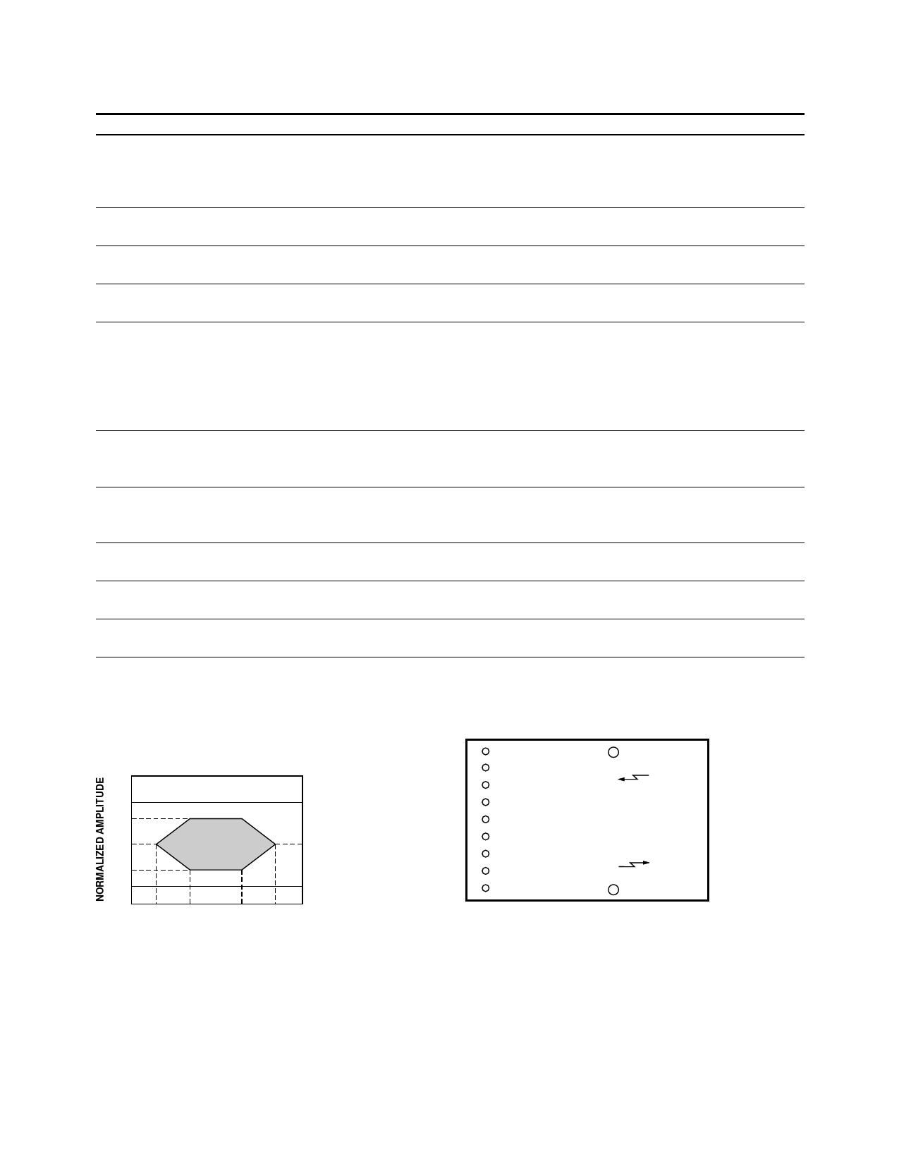
Table 1. Pinout Table
Pin Symbol Functional Description
Mounting Pins
The mounting pins are provided for transceiver mechanical attachment to the circuit board. They
are embedded in the nonconductive plastic housing and are not connected to the transceiver
internal circuit, nor is there a guaranteed connection to the metallized housing in the EM and FM
versions. They should be soldered into plated-through holes on the printed circuit board.
1
VEER
2
RD+
Receiver Signal Ground
Directly connect this pin to receiver signal ground plane. (For HFBR-53A5VM, VEER = VEET)
Receiver Data Out
AC coupled – PECL compatible.
3
RD–
Receiver Data Out Bar
AC coupled – PECL compatible.
4
SD
5
VCCR
6
VCCT
7
TD–
Signal Detect
Signal Detect is a single-ended TTL output. If Signal Detect output is not used, leave it
open-circuited.
Normal optical input levels to the receiver result in a logic “1” output, VOH, asserted.
Low input optical levels to the receiver result in a fault condition indicated by a logic “0” output
VOL, deasserted.
Receiver Power Supply
Provide +3.3 Vdc via the recommended receiver power supply filter circuit.
Locate the power supply filter circuit as close as possible to the VCCR pin.
Transmitter Power Supply
Provide +3.3 Vdc via the recommended transmitter power supply filter circuit.
Locate the power supply filter circuit as close as possible to the VCCT pin.
Transmitter Data In-Bar
AC coupled – PECL compatible. Internally terminated differentially with 100 Ω.
8
TD+
Transmitter Data In
AC coupled – PECL compatible. Internally terminated differentially with 100 Ω.
9
VEET
Transmitter Signal Ground
Directly connect this pin to the transmitter signal ground plane.
1.3
1.0
0.8
0.5
0.2
0
-0.2
0 0.22 0.375
0.625 0.78 1.0
NORMALIZED TIME
Figure 1. Transmitter Optical Eye Diagram Mask.
1 = VEER
2 = RD+
3 = RD-
4 = SD
5 = VCCR
6 = VCCT
7 = TD-
8 = TD+
9 = VEET
NIC
RX
TX
NIC
TOP VIEW
NIC = NO INTERNAL CONNECTION (MOUNTING PINS)
Figure 2. Pin-Out.
8
Share Link: