IDT72413(2003) 查看數據表(PDF) - Integrated Device Technology
零件编号
产品描述 (功能)
生产厂家
IDT72413 Datasheet PDF : 10 Pages
| |||
IDT72413 CMOS PARALLEL FIFO WITH FLAGS
64 x 5
COMMERCIAL TEMPERATURE RANGE
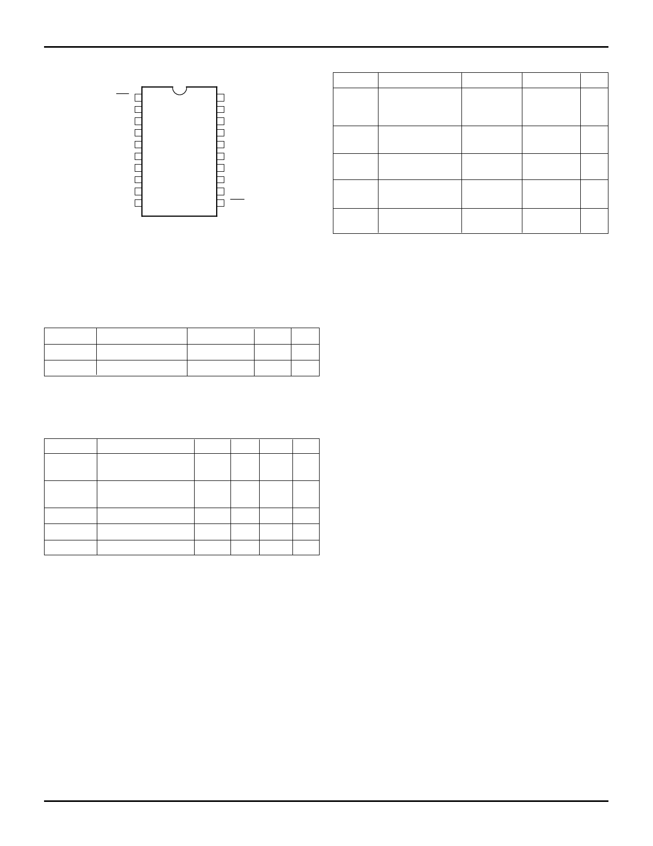
PIN CONFIGURATION
OE 1
HF 2
IR 3
SI 4
D0 5
D1 6
D2 7
D3 8
D4 9
GND 10
20 Vcc
19 AF/E
18 SO
17 OR
16 Q0
15 Q1
14 Q2
13 Q3
12 Q4
11 MR
2748 drw 02
PLASTIC DIP (P20-1, ORDER CODE: P)
SOIC (SO20-2, ORDER CODE: SO)
TOP VIEW
CAPACITANCE
(TA = +25°C, f = 1.0MHz)
Symbol
Parameter
Conditions
CIN
Input Capacitance
VIN = 0V
COUT
Output Capacitance
VOUT = 0V
NOTE:
1. Characterized values, not currently tested.
Max. Unit
5
pF
7
pF
2748 tbl 02
ABSOLUTE MAXIMUM RATINGS(1)
Symbol
VTERM
TSTG
IOUT
Rating
Commercial Unit
Terminal Voltage with –0.5 to +7.0
V
Respect to GND
Storage
–55 to +125
°C
Temperature
DC Output
–50 to +50
mA
Current
NOTE:
1. Stresses greater than those listed under ABSOLUTE MAXIMUM RATINGS may
cause permanent damage to the device. This is a stress rating only and
functional operation of the device at these or any other conditions above those
indicated in the operational sections of this specification is not implied. Exposure
to absolute maximum rating conditions for extended periods may affect reliability.
RECOMMENDED OPERATING
CONDITIONS
Symbol
Parameter
Min. Typ. Max. Unit
VCC
Supply Voltage
Commercial
4.5 5.0 5.5 V
GND
Supply Voltage
0
0 0V
VIH
VIL(1)
Input High Voltage
Input Low Voltage
2.0 — — V
— — 0.8 V
TA
Operating Temperature
Commercial
0
— 70 ° C
NOTE:
1. 1.5V undershoots are allowed for 10ns once per cycle.
DC ELECTRICAL CHARACTERISTICS
(Commercial: VCC = 5.0V ± 10%, TA = 0°C to +70°C)
IDT72413
Commercial
Symbol
Parameter
Test Conditions
fIN = 45, 35, 25 MHz
Min.
Max.
Unit
IIL
Low-Level Input Current
VCC = Max., GND ≤ VI ≤ VCC
–10
—
µA
IIH
High-Level Input Current
VCC = Max., GND ≤ VI ≤ VCC
—
10
µA
VOL Low-Level Output Current
VCC = Min. IOL (Q0-4)
24 mA
—
IOL (IR, OR)(1)
8mA
0.4
V
IOL (HF, AF/E)
8mA
VOH High-Level Output Current
VCC = Min. IOH (Q0-4)
–4mA
2.4
—
V
IOH (IR, OR)
–4mA
IOS(2) Output Short-Circuit Current
IOH (HF, AF/E) –4mA
VCC = Max. VO = 0V
–20
–110
mA
IHZ
HIGH Impedance Output Current
VCC = Max. VO = 2.4V
—
20
µA
ILZ
LOW Impedance Output Current
ICC(3,4) Active Supply Current
VCC = Max. VO = 0.4V
VCC = Max., OE = HIGH
–20
—
µA
—
60
mA
Inputs LOW, f = 25MHz
NOTES:
1. Care should be taken to minimize as much as possible the DC and capactive load on IR and OR when operating at frequencies above 25MHz.
2. Not more than one output should be shorted at a time and duration of the short circuit should not exceed one second. Guaranteed by design, but not currently tested.
3. Tested with outputs open (IOUT = 0).
4. For frequencies greater than 25MHz, ICC = 60mA + (1.5mA x [f –25MHz]) commercial.
2
Share Link: 