M5M5W816TP-55HI 查看數據表(PDF) - Renesas Electronics
零件编号
产品描述 (功能)
生产厂家
M5M5W816TP-55HI Datasheet PDF : 10 Pages
| |||
2002.08.30 Ver. 6.1
M5M5W816TP - 55HI, 70HI, 85HI
MITSUBISHI LSIs
8388608-BIT (524288-WORD BY 16-BIT) CMOS STATIC RAM
DESCRIPTION
The M5M5W816TP is a f amily of low v oltage 8-Mbit static
RAMs organized as 524288-words by 16-bit, f abricated by
Mitsubishi's high-perf ormance 0.18µm CMOS technology .
The M5M5W816TP is suitable f or memory applications
where a simple interf acing , battery operating and battery
backup are the important design objectiv es.
The M5M5W816TP is packaged in a 44pin thin small
outline mount dev ice, with the outline of 400mil TSOP
TY PE(II). It giv es the best solution f or a compaction of
mounting area as well as f lexibility of wiring pattern of
printed circuit boards.
FEATURES
- Single 2.7~3.6V power supply
- Small stand-by current: 0.1µA (2.0V, ty p.)
- No clocks, No ref resh
- Data retention supply v oltage =2.0V
- All inputs and outputs are TTL compatible.
- Easy memory expansion by S#, BC1# and BC2#
- Common Data I/O
- Three-state outputs: OR-tie capability
- OE# prev ents data contention in the I/O bus
- Process technology : 0.18µm CMOS
- Package: 44pin 400mil TSOP TYPE(II)
Version,
Operating
temperature
I-version
-40~+85°C
Part name
M5M5W816TP -55HI
M5M5W816TP -70HI
M5M5W816TP -85HI
Power
Supply
2.7~3.6V
Stand-by c urrent
Activ e
Access time * Typ. (@ 3.0V) Ratings (max. @3.6V) current
max.
Icc1
25°C 40°C 25°C 40°C 70°C 85°C *(3.0V ty p.)
55ns
70ns
85ns
0.5 1.0 5.0 8.0 20 40
30mA
(10MHz)
5mA
(1MHz)
* Typical parameter indicates the value for the
center of distribution, and not 100% tested.
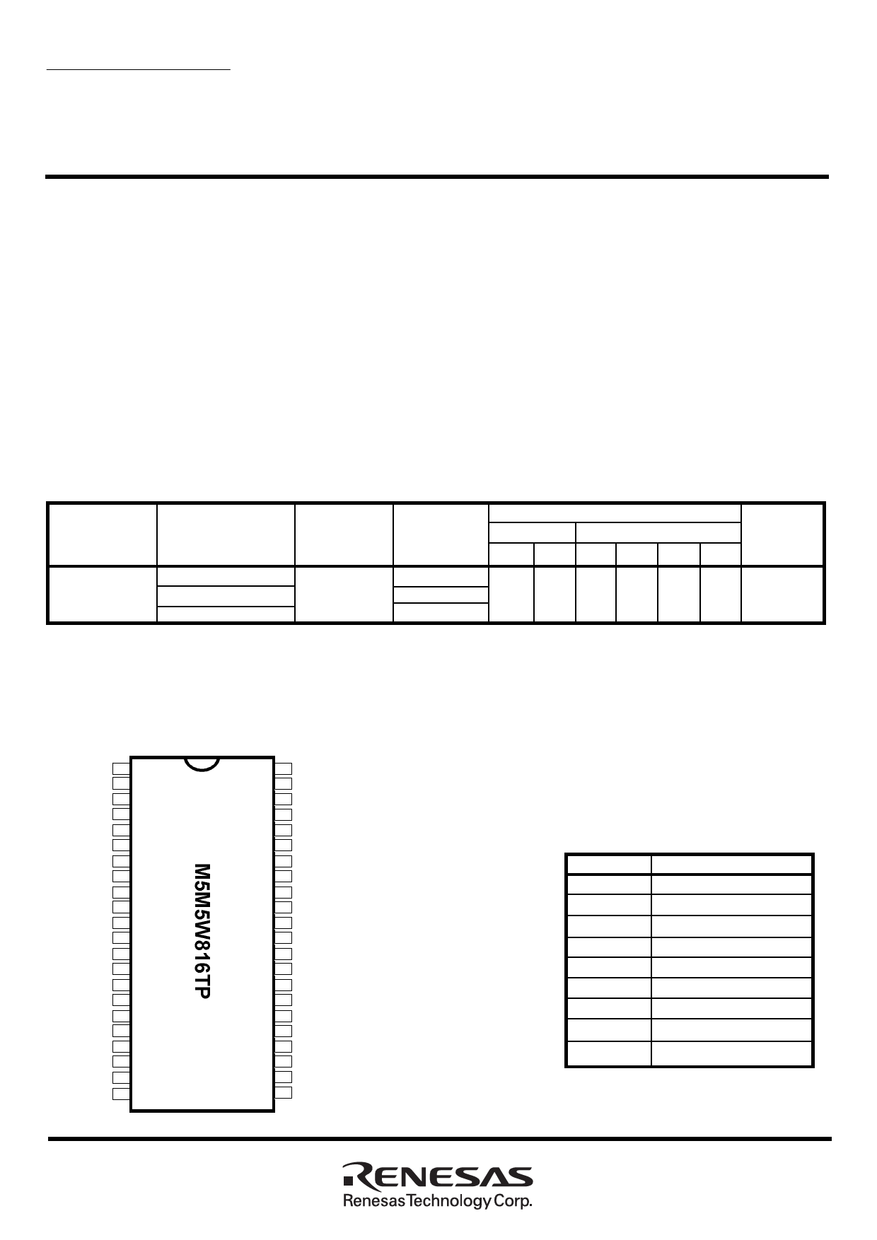
PIN CONFIGURATION
A4
1
A3
2
A2
3
A1
4
A0
5
S# 6
DQ1 7
DQ2 8
DQ3 9
DQ4 10
VCC 11
GND 12
DQ5 13
DQ6 14
DQ7 15
DQ8 16
W # 17
A15 18
A14 19
A13 20
A12 21
A16 22
44 A5
43 A6
42 A7
41 OE#
40 BC2#
39 BC1#
38 DQ16
37 DQ15
36 DQ14
35 DQ13
34 GND
33 VCC
32 DQ12
31 DQ11
30 DQ10
29 DQ9
28 A18
27 A8
26 A9
25 A10
24 A11
23 A17
44Pin 400mil TSOP
Outline: 44P3W
Pin
Function
A0 ~ A18 Address input
DQ1 ~ DQ16 Data input / output
S#
W#
OE#
Chip select input
Write control input
Output enable input
BC1#
BC2#
Lower By te (DQ1 ~ 8)
Upper By te (DQ9 ~ 16)
Vcc
Power supply
GND Ground supply
1
Share Link: 