MAX1444(2003) 查看數據表(PDF) - Maxim Integrated
零件编号
产品描述 (功能)
生产厂家
MAX1444 Datasheet PDF : 20 Pages
| |||
10-Bit, 40Msps, 3.0V, Low-Power
ADC with Internal Reference
Detailed Description
The MAX1444 uses a 10-stage, fully differential,
pipelined architecture (Figure 1) that allows for high-
speed conversion while minimizing power consump-
tion. Each sample moves through a pipeline stage
every half-clock cycle. Counting the delay through the
output latch, the clock-cycle latency is 5.5.
A 1.5-bit (2-comparator) flash ADC converts the held
input voltage into a digital code. The following digital-
to-analog converter (DAC) converts the digitized result
back into an analog voltage, which is then subtracted
from the original held input signal. The resulting error
signal is then multiplied by two, and the product is
passed along to the next pipeline stage where the
process is repeated until the signal has been
processed by all 10 stages. Each stage provides a
1-bit resolution.
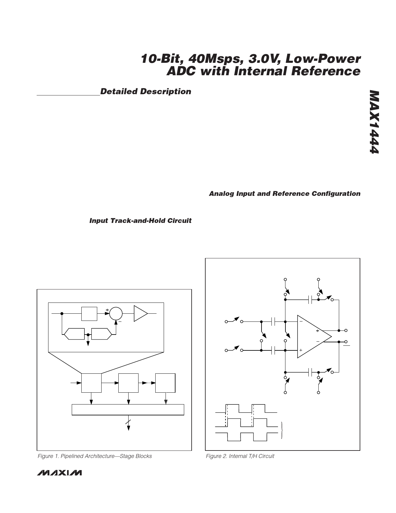
Input Track-and-Hold Circuit
Figure 2 displays a simplified functional diagram of the
input track-and-hold (T/H) circuit in both track and hold
mode. In track mode, switches S1, S2a, S2b, S4a, S4b,
S5a, and S5b are closed. The fully differential circuit
samples the input signal onto the two capacitors (C2a
and C2b). Switches S2a and S2b set the common
mode for the amplifier input. The resulting differential
MDAC
VIN
T/H
Σ
FLASH
ADC
DAC
1.5 BITS
x2
VOUT
VIN
STAGE 1
STAGE 2
STAGE 10
DIGITAL ALIGNMENT LOGIC
10
D9–D0
VIN = INPUT VOLTAGE BETWEEN
IN+ AND IN- (DIFFERENTIAL OR SINGLE-ENDED)
Figure 1. Pipelined Architecture—Stage Blocks
voltage is held on C2a and C2b. Switches S4a, S4b,
S5a, S5b, S1, S2a, and S2b are then opened before
S3a, S3b, and S4c are closed, connecting capacitors
C1a and C1b to the amplifier output. This charges C1a
and C1b to the same values originally held on C2a and
C2b. This value is then presented to the first-stage
quantizer and isolates the pipeline from the fast-chang-
ing input. The wide-input-bandwidth T/H amplifier
allows the MAX1444 to track and sample/hold analog
inputs of high frequencies beyond Nyquist. The analog
inputs (IN+ and IN-) can be driven either differentially
or single-ended. It is recommended to match the
impedance of IN+ and IN- and set the common-mode
voltage to midsupply (VDD/2) for optimum performance.
Analog Input and Reference Configuration
The MAX1444 full-scale range is determined by the
internally generated voltage difference between REFP
(VDD/2 + VREFIN/4) and REFN (VDD/2 - VREFIN/4). The
ADC’s full-scale range is user-adjustable through the
REFIN pin, which provides a high input impedance for
this purpose. REFOUT, REFP, COM (VDD/2), and REFN
are internally buffered, low-impedance outputs.
INTERNAL
BIAS
S2a
COM
S5a
C1a
S3a
S4a
IN+
OUT
C2a
S4c
S1
IN-
S4b
C2b
OUT
C1b
S3b
S2b
S5b
INTERNAL
COM
BIAS
CLK
TRACK
TRACK
HOLD
HOLD
INTERNAL
NON-OVERLAPPING
CLOCK SIGNALS
Figure 2. Internal T/H Circuit
______________________________________________________________________________________ 11
Share Link: 