MAX1444(2003) 查看數據表(PDF) - Maxim Integrated
零件编号
产品描述 (功能)
生产厂家
MAX1444 Datasheet PDF : 20 Pages
| |||
10-Bit, 40Msps, 3.0V, Low-Power
ADC with Internal Reference
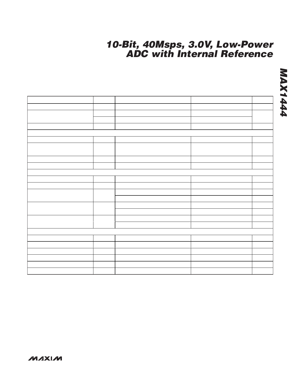
ELECTRICAL CHARACTERISTICS (continued)
(VDD = 3V; OVDD = 2.7V; 0.1µF and 1µF capacitors from REFP, REFN, and COM to GND; VREFIN = 2.048V; REFOUT connected to
REFIN through a 10kΩ resistor; VIN = 2VP-P (differential with respect to COM); CL = 10pF at digital outputs; fCLK = 40MHz; TA = TMIN
to TMAX, unless otherwise noted. ≥ +25°C guaranteed by production test, < +25°C guaranteed by design and characterization; typi-
cal values are at TA = +25°C.)
PARAMETER
Input Hysteresis
Input Leakage
Input Capacitance
DIGITAL OUTPUTS (D9–D0)
Output Voltage Low
SYMBOL
VHYST
IIH
IIL
CIN
CONDITIONS
VIH = VDD = OVDD
VIL = 0
VOL ISINK = 200µA
Output Voltage High
VOH ISOURCE = 200µA
Three-State Leakage Current
Three-State Output Capacitance
POWER REQUIREMENTS
Analog Supply Voltage
Output Supply Voltage
Analog Supply Current
Output Supply Current
Power-Supply Rejection
TIMING CHARACTERISTICS
CLK Rise to Output Data Valid
OE Fall to Output Enable
OE Rise to Output Disable
CLK Pulse Width High
CLK Pulse Width Low
Wake-up Time
ILEAK
COUT
OE = OVDD
OE = OVDD
VDD
OVDD
IVDD
IOVDD
PSRR
Operating, fIN = 19.91MHz at -0.5dBFS
Shutdown, clock idle, PD = OE = OVDD
Operating, fIN = 19.91MHz at -0.5dBFS
Shutdown, clock idle, PD = OE = OVDD
Offset
Gain
tDO
tENABLE
tDISABLE
tCH
tCL
tWAKE
Figure 6 (Note 3)
Figure 5
Figure 5
Figure 6, clock period 25ns
Figure 6, clock period 25ns
(Note 4)
MIN
TYP
0.1
5
OVDD -
0.2
5
2.7
3.0
1.7
3.0
19
4
4.5
1
±0.1
±0.1
5
10
15
12.5 ±3.8
12.5 ±3.8
1.7
MAX
±5
±5
0.2
±10
3.6
3.6
27
15
20
8
UNITS
V
µA
pF
V
V
µA
pF
V
V
mA
µA
mA
µA
mV/V
%/V
ns
ns
ns
ns
ns
µs
Note 1: SNR, SINAD, THD, SFDR, and HD3 are based on an analog input voltage of -0.5dBFS referenced to a +1.024V full-scale
input voltage range.
Note 2: Intermodulation distortion is the total power of the intermodulation products relative to the individual carrier. This number is
6dB better if referenced to the two-tone envelope.
Note 3: Digital outputs settle to VIH / VIL.
Note 4: REFIN is driven externally. REFP, COM, and REFN are left floating while powered down.
_______________________________________________________________________________________ 5
Share Link: 