MAX1446(2003) 查看數據表(PDF) - Maxim Integrated
零件编号
产品描述 (功能)
生产厂家
MAX1446 Datasheet PDF : 16 Pages
| |||
PIN
1
2
3, 9, 10
4, 5, 8, 11, 14, 30
6
7
12
13
15
16–20
21
22
23
24–28
29
31
32
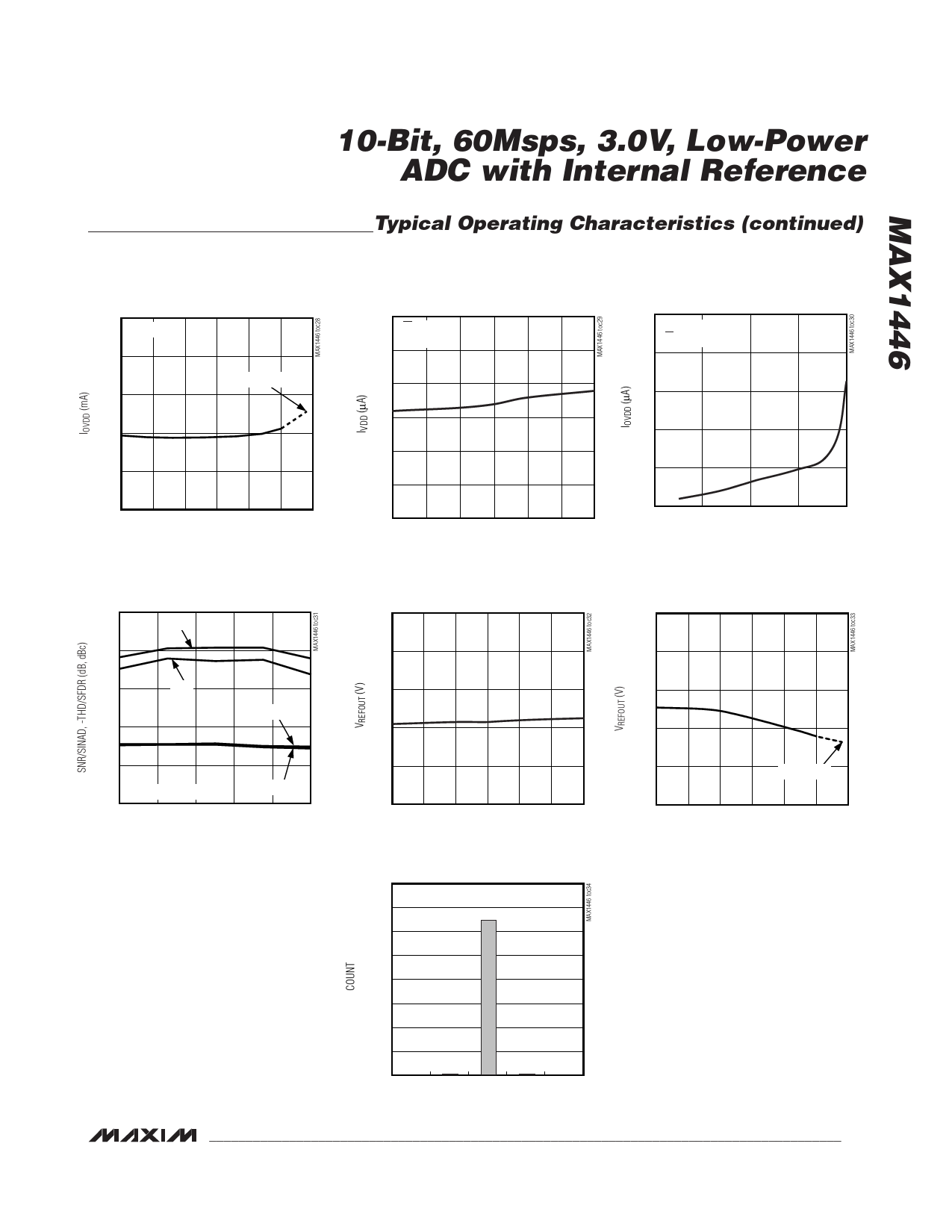
10-Bit, 60Msps, 3.0V, Low-Power
ADC with Internal Reference
NAME
REFN
COM
VDD
GND
IN+
IN-
CLK
PD
OE
D9–D5
OVDD
T.P.
OGND
D4–D0
REFOUT
REFIN
REFP
Pin Description
FUNCTION
Lower Reference. Conversion range is ±(VREFP - VREFN). Bypass to GND with a >0.1µF
capacitor.
Common-Mode Voltage Output. Bypass to GND with a >0.1µF capacitor.
Analog Supply Voltage. Bypass to GND with a capacitor combination of 2.2µF in parallel
with 0.1µF.
Analog Ground
Positive Analog Input. For single-ended operation, connect signal source to IN+.
Negative Analog Input. For single-ended operation, connect IN- to COM.
Conversion Clock Input
Power-Down Input
High: power-down mode
Low: normal operation
Output Enable Input
High: digital outputs disabled
Low: digital outputs enabled
Three-State Digital Outputs D9–D5. D9 is the MSB.
Output Driver Supply Voltage. Bypass to GND with a capacitor combination of 2.2µF in
parallel with 0.1µF.
Test Point. Do not connect.
Output Driver Ground
Three-State Digital Outputs D4–D0. D0 is the LSB.
Internal Reference Voltage Output. May be connected to REFIN through a resistor or a
resistor-divider.
Reference Input. VREFIN = 2 × (VREFP - VREFN). Bypass to GND with a >0.01µF capacitor.
Upper Reference. Conversion range is ±(VREFP - VREFN). Bypass to GND with a >0.1µF
capacitor.
_______________________________________________________________________________________ 9
Share Link: 