MAX1742 查看數據表(PDF) - Maxim Integrated
零件编号
产品描述 (功能)
生产厂家
MAX1742
Maxim Integrated

MAX1742 Datasheet PDF : 16 Pages
| |||
1A/2.7A, 1MHz, Step-Down Regulators with
Synchronous Rectification and Internal Switches
ABSOLUTE MAXIMUM RATINGS
VCC, IN to GND ........................................................-0.3V to +6V
IN to VCC.............................................................................±0.3V
GND to PGND.....................................................................±0.3V
All Other Pins to GND.................................-0.3V to (VCC + 0.3V)
LX Current (Note 1).............................................................±4.7A
REF Short Circuit to GND Duration ............................Continuous
ESD Protection .....................................................................±2kV
Continuous Power Dissipation (TA = +70°C)
SSOP (derate 16.7mW/°C above +70°C;
part mounted on 1 in.2 of 1oz. copper) ...............................1W
Operating Temperature Range ...........................-40°C to +85°C
Storage Temperature Range .............................-65°C to +150°C
Lead Temperature (soldering, 10s) ................................ +300°C
Note 1: LX has internal clamp diodes to PGND and IN. Applications that forward-bias these diodes should take care not to exceed
the IC’s package power dissipation limits.
Stresses beyond those listed under “Absolute Maximum Ratings” may cause permanent damage to the device. These are stress ratings only, and functional
operation of the device at these or any other conditions beyond those indicated in the operational sections of the specifications is not implied. Exposure to
absolute maximum rating conditions for extended periods may affect device reliability.
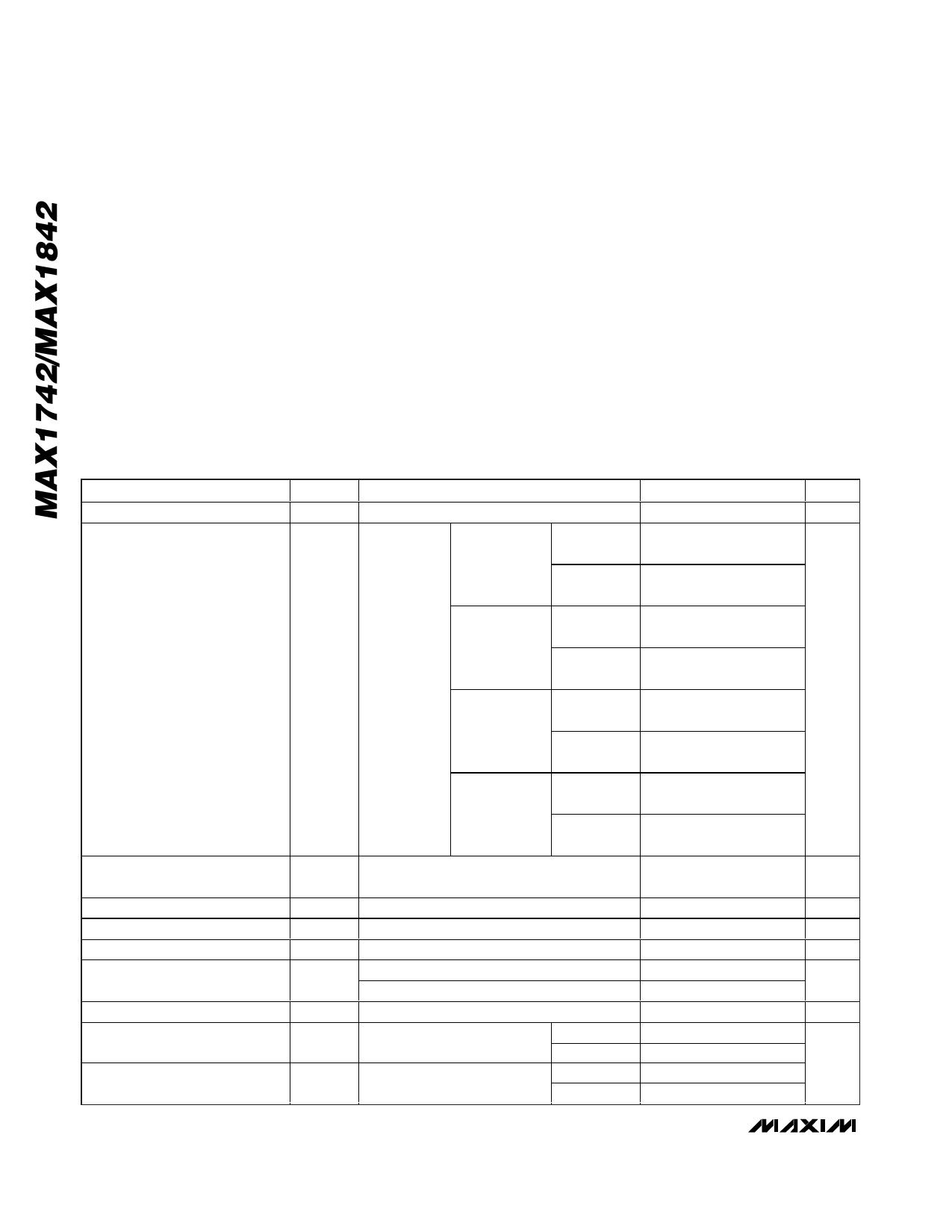
ELECTRICAL CHARACTERISTICS
(VIN = VCC = 3.3V, FBSEL = GND, TA = 0°C to +85°C, unless otherwise noted. Typical values are at TA = +25°C.)
PARAMETER
Input Voltage
SYMBOL
VIN, VCC
CONDITIONS
FBSEL =
VCC
TA = +25°C
to +85°C
TA = +0°C
to +85°C
MIN
3.0
2.500
2.487
TYP
2.525
2.525
MAX
5.5
2.550
2.563
Preset Output Voltage
VOUT
VIN = 3V to
5.5V,
ILOAD = 0
to 1A for
MAX1742,
ILOAD = 0
to 2.5A for
MAX1842,
VFB = VOUT
FBSEL =
unconnected
FBSEL =
REF
TA = +25°C
to +85°C
TA = +0°C
to +85°C
TA = +25°C
to +85°C
TA = +0°C
to +85°C
1.500
1.492
1.800
1.791
1.515
1.515
1.818
1.818
1.530
1.538
1.836
1.845
FBSEL =
GND
TA = +25°C
to +85°C
TA = +0°C
to +85°C
1.089
1.084
1.100
1.100
1.111
1.117
Adjustable Output Voltage
Range
AC Load Regulation Error
DC Load Regulation Error
Dropout Voltage
Reference Voltage
Reference Load Regulation
PMOS Switch
On-Resistance
NMOS Switch
On-Resistance
VIN = VCC = 3V to 5.5V, ILOAD = 0,
FBSEL = GND
VDO
VREF
ΔVREF
RON, P
VIN = VCC = 3V, ILOAD = 1A
TA = +25°C to +85°C
TA = +0°C to +85°C
IREF = -1µA to +10µA
ILX = 0.5A
RON, N ILX = 0.5A
VIN = 4.5V
VIN = 3V
VIN = 4.5V
VIN = 3V
VREF
1.089
1.084
2
0.4
1.100
1.100
0.5
90
110
70
80
VIN
250
1.111
1.117
2
200
250
150
200
UNITS
V
V
V
%
%
mV
V
mV
mΩ
2 _______________________________________________________________________________________
Share Link: