MAX1744 查看數據表(PDF) - Maxim Integrated
零件编号
产品描述 (功能)
生产厂家
MAX1744 Datasheet PDF : 15 Pages
| |||

High-Voltage, Step-Down DC-DC
Controllers in µMAX
ABSOLUTE MAXIMUM RATINGS
IN, EXT, SHDN to GND...........................................-0.3V to +38V
VH to GND..............................................................-0.3V to +34V
VH, EXT to IN............................................................-7V to +0.3V
CS, OUT to GND ....................................................-0.3V to +20V
FB, 3/5, REF to GND .....................................-0.3V to (VL + 0.3V)
VL to GND...................................................................-0.3V to 6V
Continuous Power Dissipation (TA = +70°C)
10-Pin μMAX (derate 5.6mW/°C above 70°C) .............444mW
Operating Temperature Range
MAX174_EUB ..................................................-40°C to +85°C
MAX174_AUB ................................................-40°C to +125°C
Junction Temperature ......................................................+150°C
Storage Temperature Range .............................-65°C to +150°C
Lead Temperature (soldering, 10s) ................................+300°C
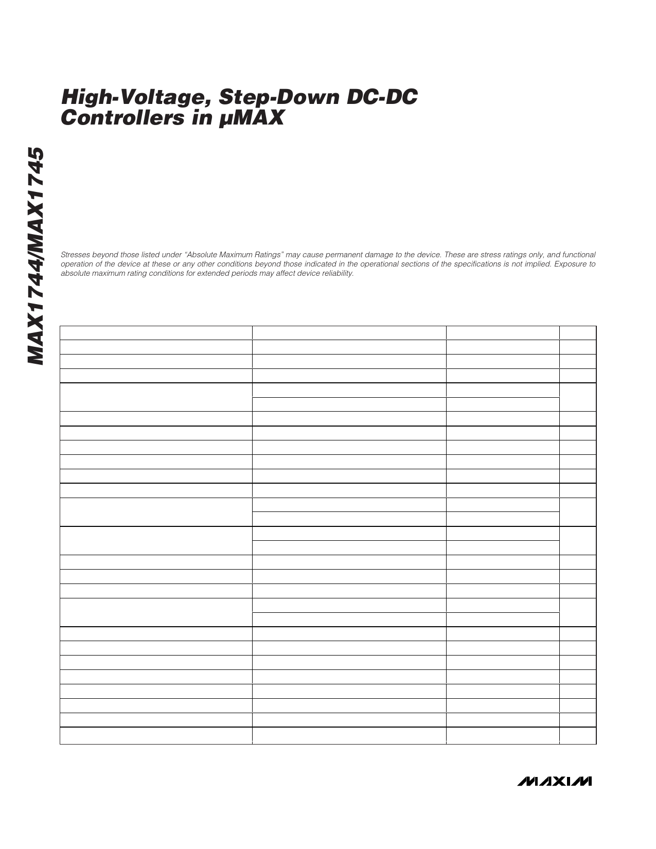
Stresses beyond those listed under “Absolute Maximum Ratings” may cause permanent damage to the device. These are stress ratings only, and functional
operation of the device at these or any other conditions beyond those indicated in the operational sections of the specifications is not implied. Exposure to
absolute maximum rating conditions for extended periods may affect device reliability.
ELECTRICAL CHARACTERISTICS
(VIN = VSHDN = 5.5V to 36V, 3/5 = GND, ILOAD = 0, TA = 0°C to +85°C, unless otherwise noted. Typical values at VIN = VSHDN =
36V, TA = +25°C.)
PARAMETER
CONDITIONS
MIN TYP MAX UNITS
Input Voltage Range
4.5
36
V
Supply Current into IN
Shutdown Supply Current
VSHDN = VIN = 5.5V to 36V
SHDN = GND
90
140
μA
4
12
μA
Output Voltage (MAX1744)
3/5 = VL
3/5 = GND
4.85 5.00 5.15
V
3.20 3.30 3.40
OUT Input Current (MAX1744)
FB Threshold Voltage (MAX1745)
3/5 = VL, VOUT = 5V
Falling edge, hysteresis = 8mV
28
44
μA
1.22 1.25 1.28
V
FB Input Current (MAX1745)
VH Output Voltage with Respect to IN
VL Output Voltage
VL Undervoltage Lockout
VIN = 5.5V to 36V, IVH = 100μA to 20mA
VIN = 5.5V to 36V, IVL = 100μA to 2mA
-50
50
nA
-6.0 -5.3 -4.3
V
4.5
5.0
5.5
V
2.0
3.0
4.1
V
CS Threshold Voltage
CS Input Current
SHDN, 3/5 Logic-High Threshold
SHDN, 3/5 Logic-Low Threshold
3/5 Input Current
VCS = VOUT = 2.5V to 18V
VCS = VOUT = VGND
VCS = VOUT = 2.5V to 18V
VCS = VOUT = VGND
VIN = 4.5V to 36V
VIN = 4.5V to 36V
SHDN = GND
85
100 115
mV
80
110 150
0
15
25
μA
-25
0
2.4
V
0.4
V
±1
μA
SHDN Input Current
EXT Resistance
3/5 = GND
VSHDN = 36V
±1
μA
12
8
20
Ω
Minimum EXT Off-Time
Minimum EXT On-Time
1.5
2.0
2.5
μs
0.7
1.0
1.5
μs
Output Line Regulation
Output Load Regulation
Reference Voltage
REF Load Regulation
REF Line Regulation
Figure 1, 5.5V < VIN < 36V, ILOAD = 1A
Figure 1, VIN = 12V, 30mA < ILOAD < 2A
IREF = 0
0 ≤ IREF ≤ 100μA
VIN = 4.5V to 36V, IREF = 0
5
mV/V
15
mV/A
1.22 1.25 1.28
V
4
10
mV
30
60
μV/V
2 _______________________________________________________________________________________