MAX1763(2001) 查看數據表(PDF) - Maxim Integrated
零件编号
产品描述 (功能)
生产厂家
MAX1763 Datasheet PDF : 16 Pages
| |||
1.5A, Low-Noise, 1MHz, Step-Up
DC-DC Converter
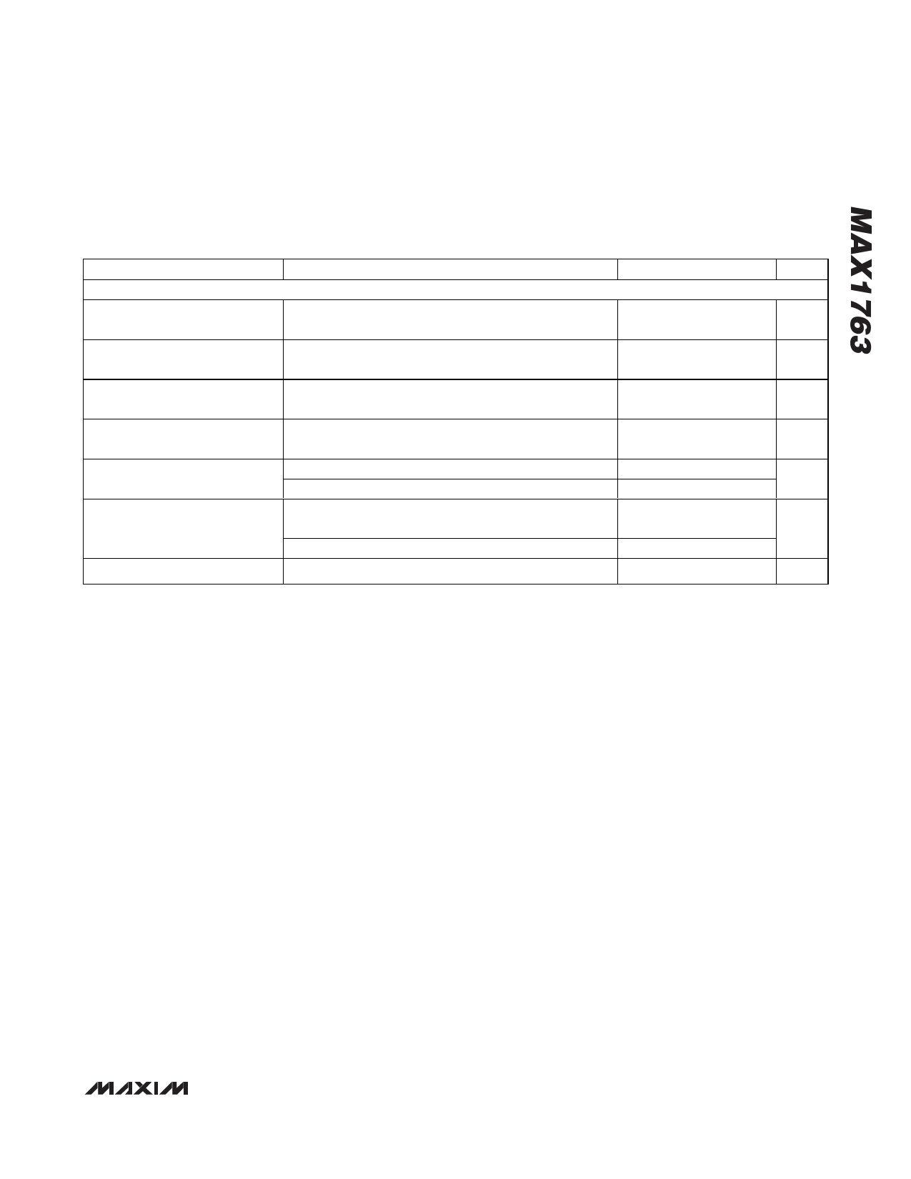
ELECTRICAL CHARACTERISTICS (continued)
(CLK/SEL = ONB = FB = PGND = GND, ISET = REF, OUT = POUT, VONA = VAIN = VOUT = 3.6V, TA = -40°C to +85°C, unless other-
wise noted.) (Note 8)
PARAMETER
LOGIC INPUTS
CONDITIONS
MIN
MAX UNITS
Gain-Block Enable Threshold
(VOUT - VAIN) (Note 6)
1.4
V
Gain-Block Disable Threshold
(VOUT - VAIN) (Note 6)
0.2
V
CLK/SEL Input Low Level
2.5 V ≤ VOUT ≤ 5.5V
(0.2)
V
VOUT
CLK/SEL Input High Level
ONA and ONB Input Low Level
(Note 7)
ONA and ONB Input High Level
(Note 7)
Input Leakage Current
2.5 V ≤ VOUT ≤ 5.5V
1.1 V ≤ VOUT ≤ 1.8V
1.8 V ≤ VOUT ≤ 5.5V
1.1 V ≤ VOUT ≤ 1.8V
1.8V ≤ VOUT ≤ 5.5V
CLK/SEL, ONA, ONB
(0.8)
VOUT
VOUT
- 0.2V
1.6
V
0.2
V
0.4
V
1
µA
Note 1: Operating voltage. Because the regulator is bootstrapped to the output, once started, the MAX1763 will operate down to
0.7V input.
Note 2: Startup is tested with the circuit of Figure 2.
Note 3: Defines low-noise mode maximum step-up ratio.
Note 4: The regulator is in startup mode until this voltage is reached. Do not apply full load current until the output exceeds 2.3V.
Note 5: Supply current from the 3.3V output is measured between the 3.3V output and the OUT pin. This current correlates directly
to the actual battery-supply current, but is reduced in value according to the step-up ratio and efficiency. The gain block is
disabled.
Note 6: Connect AIN to OUT to disable gain block.
Note 7: ONA and ONB have hysteresis of approximately 0.15 ✕ VOUT.
Note 8: Specifications to -40°C are guaranteed by design and not production tested.
_______________________________________________________________________________________ 5
Share Link: 