MAX1800EHJ 查看數據表(PDF) - Maxim Integrated
零件编号
产品描述 (功能)
生产厂家
MAX1800EHJ Datasheet PDF : 24 Pages
| |||
Digital Camera Step-Up
Power Supply
ABSOLUTE MAXIMUM RATINGS
OUT, POUT, ON_, DCON_, FB_, RDYM to GND .....-0.3V to +6.0V
PGND to GND ......................................................-0.3V to +0.3V
OUT to POUT_ ......................................................-0.3V to +0.3V
LX, DL_, AO to PGND .............................-0.3V to (POUT + 0.3V)
REF, OSC, AI, COMP_ to GND..................-0.3V to (OUT + 0.3V)
Continuous Power Dissipation (TA = +70°C)
32-Pin TQFP (derate 11mW/°C above +70°C) ............880mW
Operating Temperature Range
MAX1800EHJ.................................................. -40°C to +85°C
Junction Temperature ......................................................+150°C
Storage Temperature Range. ............................-65°C to +150°C
Lead Temperature (soldering, 10s) .................................+300°C
Stresses beyond those listed under “Absolute Maximum Ratings” may cause permanent damage to the device. These are stress ratings only, and functional
operation of the device at these or any other conditions beyond those indicated in the operational sections of the specifications is not implied. Exposure to
absolute maximum rating conditions for extended periods may affect device reliability.
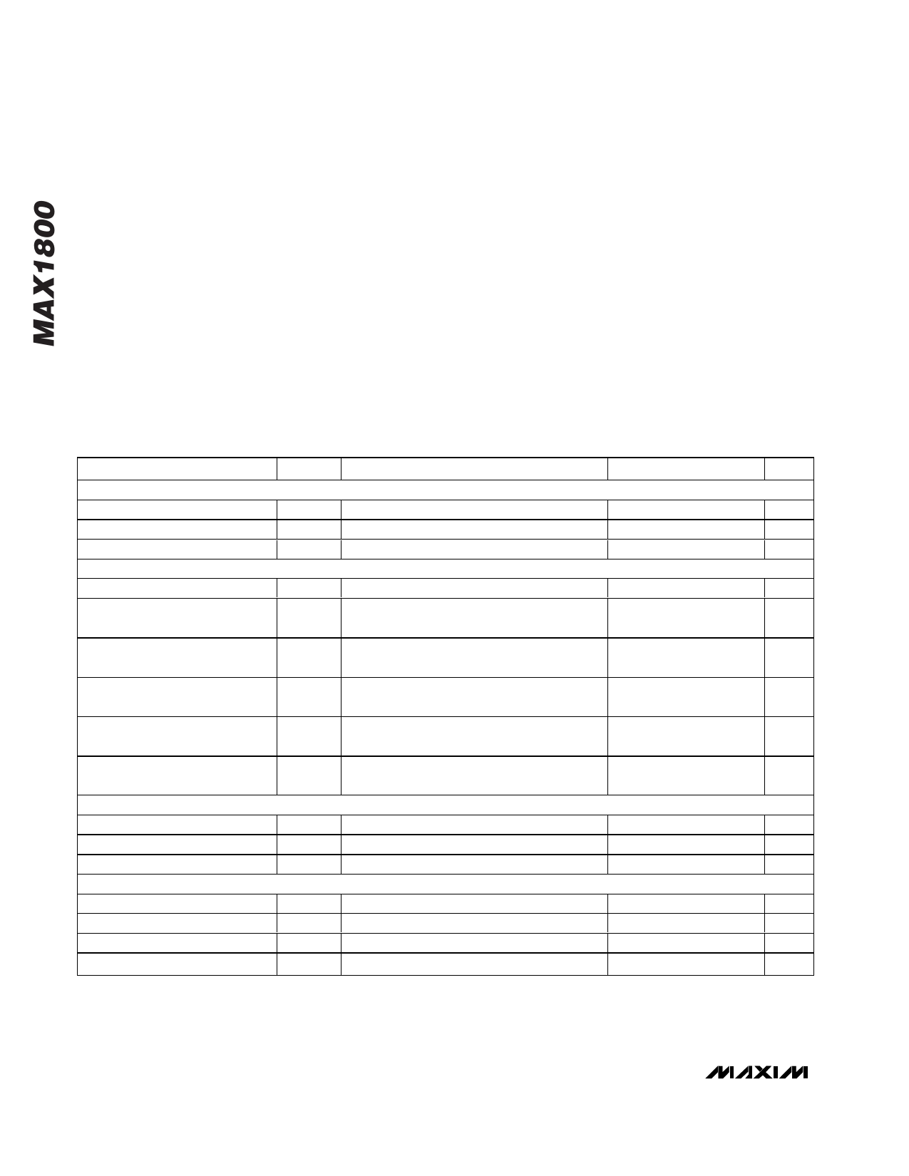
ELECTRICAL CHARACTERISTICS
(Circuit of Figure 1, VOUT = VPOUT = 3.3V, PGND = GND, VONM = 3.3V, VON1 = VON2 = VON3 = VONA = 0, TA = -40°C to +85°C,
unless otherwise noted. Typical values are at TA = +25°C.) (Note 1)
PARAMETER
GENERAL
Input Voltage Range (Note 2)
Minimum Startup Voltage
Frequency in Startup Mode
SUPPLY CURRENT
Shutdown Supply Current
Main DC/DC Converter Supply
Current
SYMBOL
CONDITIONS
VIN
VSTART
ILOAD < 1mA, TA = +25oC
VOUT = 1.5V
VONM = 0
VFBM = 1.2V, VOSC = 0
MIN TYP MAX UNITS
0.7
5.5
V
0.9
1.1
V
40
150 300 kHz
0.002
5
µA
250 400
µA
Main + Auxiliary 1 Supply
Current
Main + Auxiliary 2 Supply
Current
Main + Auxiliary 3 Supply
Current
Analog Gain Block Supply
Current
REFERENCE
Reference Output Voltage
REF Load Regulation
REF Line Rejection
OSCILLATOR
OSC Discharge Trip Level
OSC Input Bias Current
OSC Discharge Resistance
OSC Discharge Pulse Width
VON1 = 3.3V, VFBM = 1.2V, VFB1 = 1.2V,
VOSC = 0
VON2 = 3.3V, VFBM = 1.2V, VFB2 = 1.2V,
VOSC = 0
VON3 = 3.3V, VFBM = 1.2V, VFB3 = 1.2V,
VOSC = 0
VONA = 3.3V, VFBM = 1.2V, AI = REF,
AO open, VOSC = 0
VREF
IREF = 20µA
10µA < IREF < 200µA
2.7V < VOUT < 5.5V
Rising edge
VOSC = 1.1V
VOSC = 1.5V, IOSC = 3mA
375 600
µA
375 600
µA
375 600
µA
375 600
µA
1.23 1.250 1.27
V
10
mV
0.2
5
mV
1.225 1.250 1.275
V
0.01 100
nA
37
75
Ω
100
ns
2 _______________________________________________________________________________________
Share Link: 