MAX17035(2009) 查看數據表(PDF) - Maxim Integrated
零件编号
产品描述 (功能)
生产厂家
MAX17035 Datasheet PDF : 27 Pages
| |||
High-Frequency,
Low-Cost SMBus Chargers
ABSOLUTE MAXIMUM RATINGS
DCIN, CSSP, BATT, CSIP to GND......................... -0.3V to +28V
CSIP to CSIN, CSSP to CSSN............................... -0.3V to +0.3V
VCC, SCL, SDA, VAA, EN, ACIN, ITHR,
ADAPTLIM, ACOK to GND................................... -0.3V to +6V
PDSL to GND......................................................... -0.3V to +37V
GND to PGND ...................................................... -0.3V to +0.3V
DHI to LX...................................................-0.3V to (VBST + 0.3V)
BST to LX................................................................. -0.3V to +6V
BST to GND............................................................ -0.3V to +34V
DLO to PGND........................................... -0.3V to (VLDO + 0.3V)
LX to GND ................................................................ -6V to +28V
CC, IINP to GND...................................... -0.3V to (VLDO + 0.3V)
LDO Short Circuit to GND.......................................... Momentary
Continuous Power Dissipation (TA = +70NC)
24-Pin, 4mm x 4mm Thin QFN
(derate 20.8mW/NC above +70NC).............................1666mW
Operating Temperature Range........................... -40NC to +85NC
Junction Temperature......................................................+150NC
Storage Temperature Range............................ -65NC to +150NC
Lead Temperature (soldering, 10s).................................+300NC
Stresses beyond those listed under “Absolute Maximum Ratings” may cause permanent damage to the device. These are stress ratings only, and functional
operation of the device at these or any other conditions beyond those indicated in the operational sections of the specifications is not implied. Exposure to absolute
maximum rating conditions for extended periods may affect device reliability.
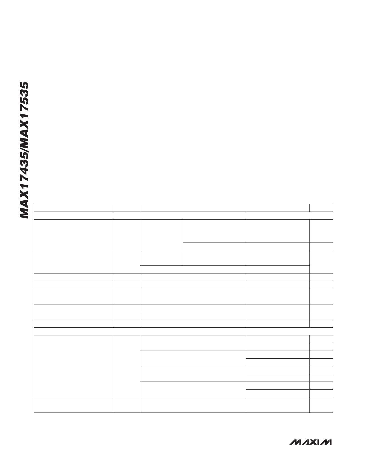
ELECTRICAL CHARACTERISTICS
(Circuit of Figure 1, no load on LDO, VDCIN = VCSSP = VCSSN = 19V, VLX = 0V, VBST - VLX = 5V, VBATT = VCSIP = VCSIN = 16.8V,
TA = 0°C to +85°C, unless otherwise noted. Typical values are at TA = +25°C.)
PARAMETER
INPUT SUPPLIES
SYMBOL
CONDITIONS
Adapter Present Quiescent
Current (Note 1)
IDCIN + ICSSP +
ICSSN + IVCC
Charging enabled,
VADAPTER = 19V,
VBATTERY = 16.8V
Charging disabled
BATT + CSIP + CSIN +
LX Input Current
VBATT = 16.8V
Adapter absent or
charger shut down
(Note 1)
DCIN Input Current
VCC Supply Current
DCIN Input-Voltage Range
for Charger
IDCIN
ICC
VBATT = 2V to 19V, adapter present (Note 1)
Charger disabled
Charger added
DCIN Undervoltage-Lockout
Trip Point for Charger
DCIN Input-Voltage Range
CHARGE-VOLTAGE REGULATION
VDCIN falling
VDCIN rising
ChargingVoltage() = 0x41A0
Battery Full-Charge Voltage
and Accuracy
ChargingVoltage() = 0x3130
ChargingVoltage() = 0x20D0
Battery Undervoltage-Lockout
Trip Point for Trickle Charge
ChargingVoltage() = 0x1060
MIN TYP MAX
3
6
1.5
2.2
1.5
200 650
0.7
1.0
1.5
2.5
8
26
7
7.2
7.7
7.9
8
24
16.733
-0.4
12.516
-0.6
8.333
-0.8
4.15
-1.0
16.8
12.592
8.4
4.192
16.867
+0.4
12.668
+0.6
8.467
+0.8
4.234
+1.0
3
3.5
4
UNITS
mA
mA
FA
mA
mA
V
V
V
V
%
V
%
V
%
V
%
V
2 _______________________________________________________________________________________
Share Link: 