MAX3397E وں¥çœ‹و•¸و“ڑè،¨ï¼ˆPDF) - Maxim Integrated
零ن»¶ç¼–هڈ·
ن؛§ه“پوڈڈè؟° (هٹں能)
ç”ںن؛§هژ‚ه®¶
MAX3397E Datasheet PDF : 13 Pages
| |||
Dual Bidirectional Low-Level
Translator in آµDFN
VL
VCC
VL VCC
EN
MAX3397E
I/O VL_
DATA
I/O VCC_
GND
RLOAD
CLOAD
VL
VCC
CLOAD
VL VCC
EN
MAX3397E
DATA
I/O VL_
I/O VCC_
RLOAD
GND
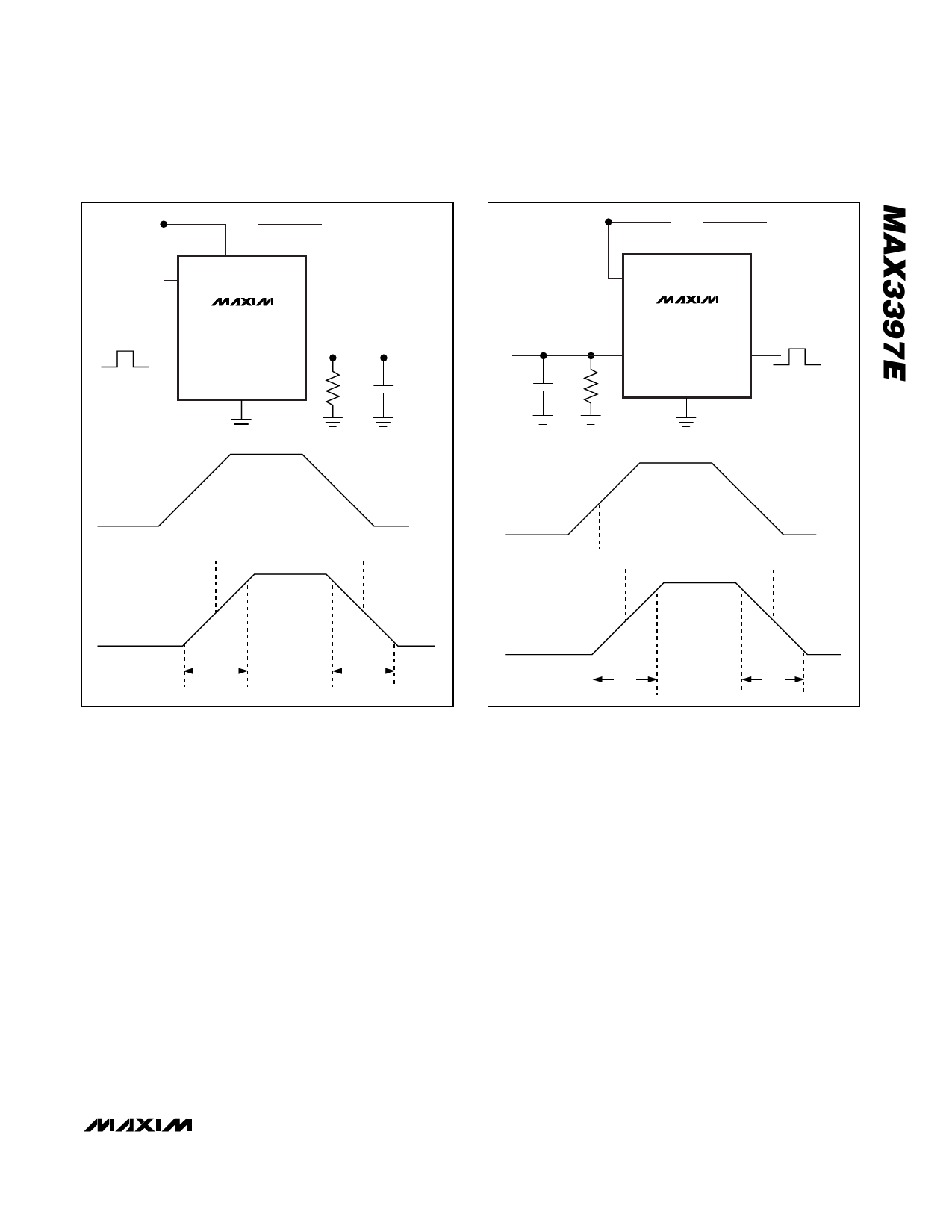
I/O VL_
(tRISE,
tFALL < 10ns)
tPD-VL-VCC
tPD-VL-VCC
I/O VCC_
(tRISE,
tFALL < 10ns)
tPD-VCC-VL
tPD-VCC-VL
I/O VCC_
I/O VL_
tRVCC
tFVCC
tRVL
tFVL
Figure 1a. Rail-to-Rail Driving I/O VL
Figure 1b. Rail-to-Rail Driving I/O VCC
Level Translation
For proper operation, ensure that +1.65V ≤ VCC ≤ +5.5V
and +1.2V ≤ VL ≤ +5.5V. During power-up sequencing,
VL ≥ (VCC + 0.3V) does not damage the device. The
speed-up circuitry limits the maximum data rate for the
MAX3397E to 16Mbps. The maximum data rate also
depends heavily on the load capacitance (see the
Typical Operating Characteristics), output impedance of
the driver, and the operational voltage range (see the
Timing Characteristics table).
Rise-Time Accelerators
The MAX3397E has an internal rise-time accelerator,
allowing operation up to 16Mbps. The rise-time accelera-
tors are present on both sides of the device and act to
speed up the rise time of the input and output of the
device, regardless of the direction of the data. The trig-
gering mechanism for these accelerators is both level
and edge sensitive. To prevent false triggering of the
rise-time accelerators, signal fall times of less than
20ns/V are recommended for both the inputs and outputs
of the device. Under less noisy conditions, longer signal
fall times are acceptable. Note: To guarantee operation
of the rise time, accelerators the maximum parasitic
capacitance should be less than 200pF on the I/O lines.
Shutdown Mode
Drive EN low to place the MAX3397E in shutdown
mode. Connect EN to VL or VCC (logic-high) for normal
operation. Activating the shutdown mode disconnects
the internal 10kΩ pullup resistors on the I/O VCC and
I/O VL lines. This forces the I/O lines to a high-imped-
ance state, and decreases the supply current to less
than 1آµA. The high-impedance I/O lines in shutdown
mode allow for use in a multidrop network. The
MAX3397E effectively has a diode from each I/O to the
corresponding supply rail and GND. Therefore, when in
shutdown mode, do not allow the voltage at I/O VL_ to
exceed (VL + 0.3V), or the voltage at I/O VCC_ to
exceed (VCC + 0.3V).
_______________________________________________________________________________________ 7
Share Link: 