MAX3991 查看數據表(PDF) - Maxim Integrated
零件编号
产品描述 (功能)
生产厂家
MAX3991 Datasheet PDF : 12 Pages
| |||
10Gbps Clock and Data Recovery
with Limiting Amplifier
PLL Retimer
The integrated PLL recovers a synchronous clock,
which is used to retime the input data. Connect a
0.047µF capacitor between CFIL and VCC to provide
PLL dampening. The external reference connected to
REFCLK aids in frequency acquisition. Because the ref-
erence clock is only used for frequency acquisition, a
low-quality reference clock can be used with no penalty
in performance. The reference clock should be within
±100ppm of the bit rate divided by 16 or 64.
Loss-of-Lock Monitor
The LOL output indicates that the frequency difference
between the recovered clock and the reference clock is
excessive. LOL may assert due to excessive jitter at the
data input, incorrect frequency, or loss of input data.
The LOL detector monitors the frequency difference
between the recovered clock and the reference clock.
The LOL output is asserted high when the frequency
difference exceeds 650ppm.
Loss-of-Signal Monitor
The LOS output indicates low, receive-signal power.
The LOS output is asserted high when the input signal
is below the threshold set by VTH.
VTH = 10 x VLOS_ASSERT(mVP-P) (typ)
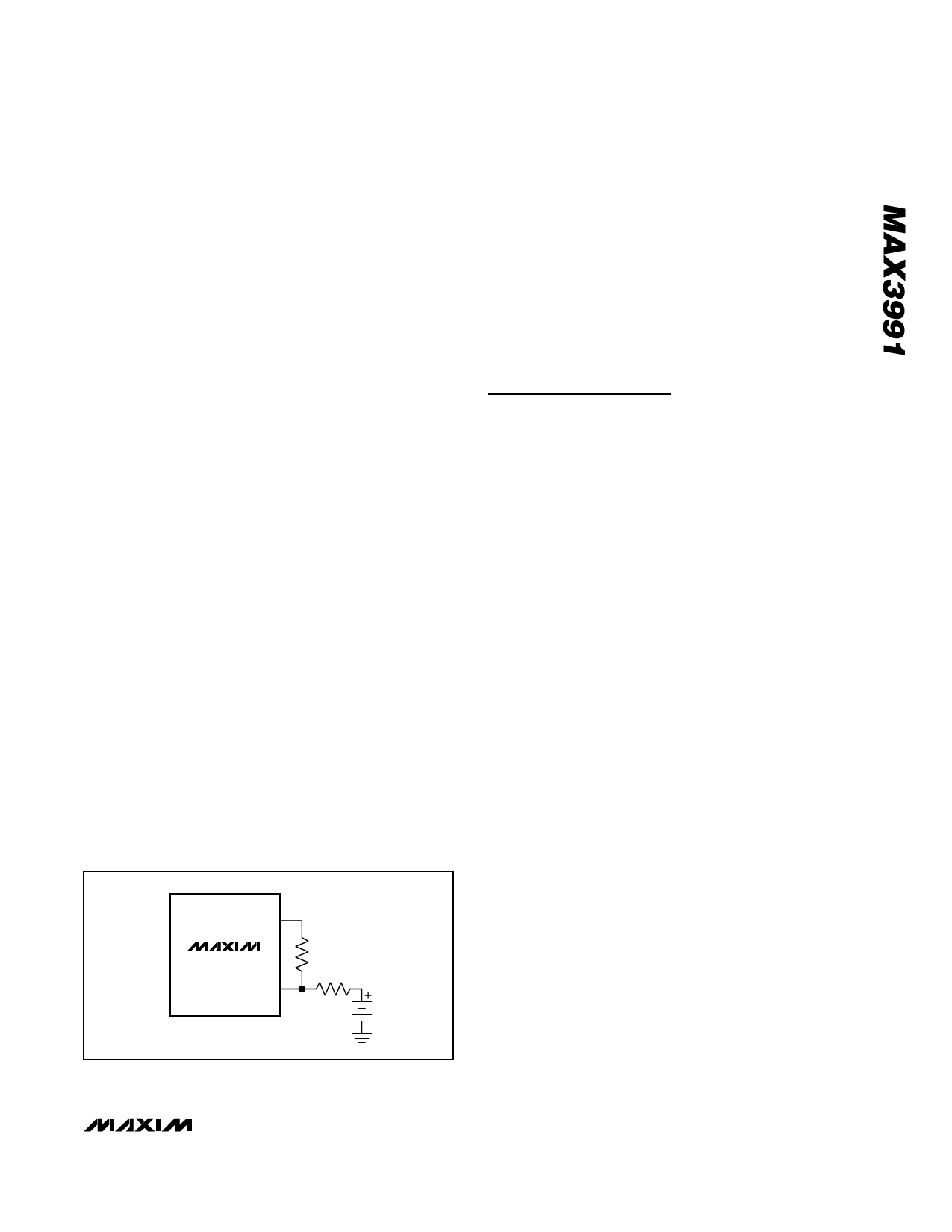
The hysteresis value of the LOS detector is internally
fixed at 1.5. Hysteresis values above 1.5 can be
achieved using external resistors as shown in Figure 4.
The new hysteresis value is:
Hysteresis = 1.5 × 3 × R1 + VREF × R2
0.2 × R1 + VREF × R2
Resistor R2 is selected to prevent loading of the LOS
pin. A value of >40kΩ is recommended. Refer to appli-
cations note HFDN 34-0.
LOS
MAX3992
VTH
R2
R1
VREF
Reference Clock Input
The REFCLK inputs are internally terminated and self-
biased to allow AC-coupling. The input impedance is
100Ω single-ended (200Ω differential). The REFCLK
inputs of the MAX3991 and MAX3992 should be con-
nected close together in parallel. The impedance look-
ing into the parallel combination is 100Ω differential.
This allows both the MAX3991 and MAX3992 to easily
interface with one reference clock without using addi-
tional components. See Figure 5.
Design Procedure
Modes of Operation
The MAX3991 has a standby mode, jitter test mode,
and squelch mode in addition to its normal operating
mode. Standby is used to conserve power. In the
standby mode, the power consumption of the MAX3991
falls below 40% of the normal-operation power con-
sumption. The jitter test mode enables the SCLK out-
puts to clock a BERT when testing jitter generation,
jitter transfer, and jitter tolerance. In the squelch mode,
the SDO± outputs are held static at VCC. The FCTL1
and FCTL2 TTL inputs are used to select the mode of
operation as shown in Table 3.
Serial Data Rate and
Reference Clock Frequency
Input Configuration
The SDI± inputs of the MAX3991 are current-mode
logic (CML) compatible. The inputs have internal 50Ω
terminations for minimum external components. See
Figure 6 for the input structure. AC-coupling is recom-
mended. The common-mode levels of DC-coupled
parts must be matched. For additional information on
logic interfacing, refer to Maxim Application Note HFAN
1.0: Introduction to LVDS, PECL, and CML.
Output Configuration
The MAX3991 uses CML for its high-speed digital out-
puts (SDO± and SCLKO±). The configuration of the out-
put circuit includes internal 50Ω back terminations to
VCC. See Figure 7 for the output structure. CML outputs
may be terminated by 50Ω to VCC, or by 100Ω differen-
tial impedance. The relation of the output polarity to input
can be reversed using the POL pin (see Figure 8).
For additional information on logic interfacing, refer to
Maxim Application Note HFAN 1.0: Introduction to LVDS,
PECL, and CML.
Figure 4. Added Hysteresis Circuit
_______________________________________________________________________________________ 9
Share Link: 