MAX4194(1999) 查看數據表(PDF) - Maxim Integrated
零件编号
产品描述 (功能)
生产厂家
MAX4194
(Rev.:1999)
(Rev.:1999)
Maxim Integrated

MAX4194 Datasheet PDF : 12 Pages
| |||
Micropower, Single-Supply, Rail-to-Rail,
Precision Instrumentation Amplifiers
ABSOLUTE MAXIMUM RATINGS
Supply Voltage (VCC to VEE)..................................................+8V
All Other Pins .................................. (VCC + 0.3V) to (VEE - 0.3V)
Current into Any Pin..........................................................±30mA
Output Short-Circuit Duration (to VCC or VEE)........... Continuous
Continuous Power Dissipation (TA = +70°C)
SO (derate 5.9mW/°C above +70°C) ........................... 471mW
Operating Temperature Range ...........................-40°C to +85°C
Junction Temperature ......................................................+150°C
Storage Temperature Range .............................-65°C to +150°C
Lead Temperature (soldering, 10sec) ............................ +300°C
Stresses beyond those listed under “Absolute Maximum Ratings” may cause permanent damage to the device. These are stress ratings only, and functional
operation of the device at these or any other conditions beyond those indicated in the operational sections of the specifications is not implied. Exposure to
absolute maximum rating conditions for extended periods may affect device reliability.
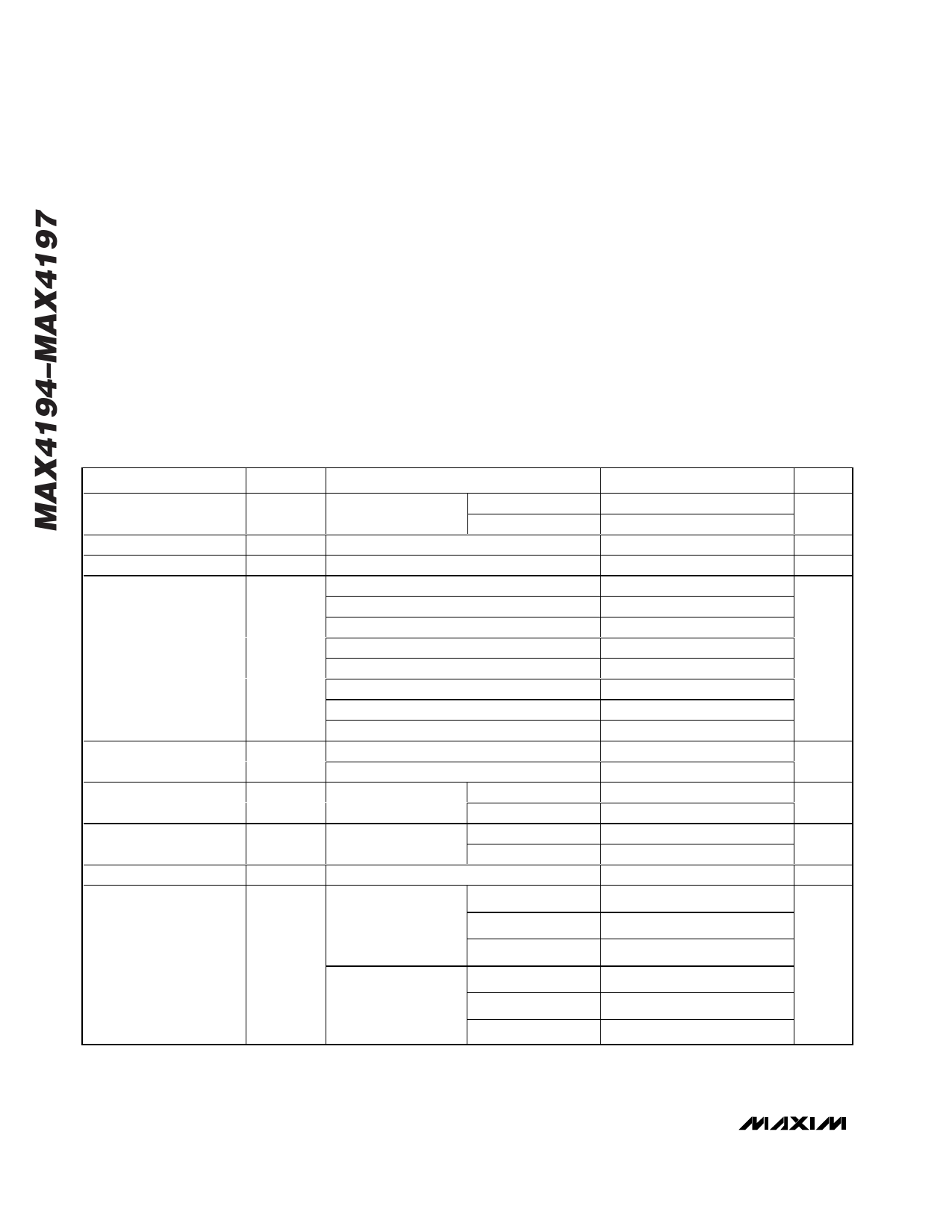
ELECTRICAL CHARACTERISTICS
(VCC = +5V, VEE = 0, RL = 25kΩ tied to VCC/2, VREF = VCC/2, TA = TMIN to TMAX, unless otherwise noted. Typical values are at
TA = +25°C.)
PARAMETER
SYMBOL
CONDITIONS
MIN TYP MAX UNITS
Supply Voltage Range
Inferred by PSR
VCC test
Single supply
Dual supplies
2.7
±1.35
7.5
V
±3.75
Quiescent Current
Shutdown Current
Input Offset Voltage
Input Offset Voltage Drift
(Note 1)
ICC
I SHDN
VOS
TCVOS
VIN+ = VIN- = VCC/2, VDIFF = 0
I SHDN = VIL, MAX4195/96/97 only
G = +1V/V, VCM = VCC/2, TA = +25°C
G = +10V/V, VCM = VCC/2, TA = +25°C
G = +100V/V, VCM = VCC/2, TA = +25°C
G = +1000V/V, VCM = VCC/2, TA = +25°C
G = +1V/V, VCM = VCC/2, TA = TMIN to TMAX
G = +10V/V, VCM = VCC/2, TA = TMIN to TMAX
G = +100V/V, VCM = VCC/2, TA = TMIN to
G = +1000V/V, VCM = VCC/2, TA = TMIN to
G = +1V/V
G ≥ +10V/V
93
8
±100
±75
±50
±50
±100
±75
±50
±50
±1.0
±0.5
110
12
±450
±225
±225
±690
±345
±345
±4.0
±2.0
µA
µA
µV
µV/°C
Input Resistance
RIN
VCM = VCC/2
Differential
Common mode
1000
MΩ
1000
Input Capacitance
CIN
VCM = VCC/2
Differential
Common mode
1
pF
4
Input Voltage Range
DC Common-Mode Rejection
VIN
CMRDC
Inferred from CMR test
VCM = VEE + 0.2V
to VCC - 1.1V,
TA = +25°C,
∆RS = 1kΩ
G = +1V/V
G = +10V/V
G = +100V/V
G = +1000V/V
VCM = VEE + 0.2V
to VCC - 1.1V,
TA = TMIN to TMAX,
∆RS = 1kΩ
G = +1V/V
G = +10V/V
G = +100V/V
G = +1000V/V
VEE + 0.2
VCC - 1.1
V
78
95
93
115
95
115
115
dB
73
95
88
115
90
115
115
AC Common-Mode Rejection
CMRAC
VCM = VEE + 0.2V
to VCC - 1.1V,
f = 120Hz
G = +1V/V
G = +10V/V
G = +100V/V
85
101
dB
106
2 _______________________________________________________________________________________
Share Link: