MAX4194 查看數據表(PDF) - Maxim Integrated
零件编号
产品描述 (功能)
生产厂家
MAX4194
Maxim Integrated

MAX4194 Datasheet PDF : 13 Pages
| |||
Micropower, Single-Supply, Rail-to-Rail,
Precision Instrumentation Amplifiers
Table 1. MAX4194 External Gain Resistor
Selection
GAIN (V/V)
CLOSEST RG (1%) CLOSEST RG (5%)
(Ω)
(Ω)
+1
∞*
∞*
+2
49.9k
51k
+5
12.4k
12k
+10
5.62k
5.6k
+20
2.61k
2.7k
+50
1.02k
1.0k
+100
511
510
+200
249
240
+500
100
100
+1,000
49.9
51
+2,000
24.9
24
+5,000
10
10
+10,000
4.99
5.1
*Leave pins 1 and 8 open for G = +1V/V.
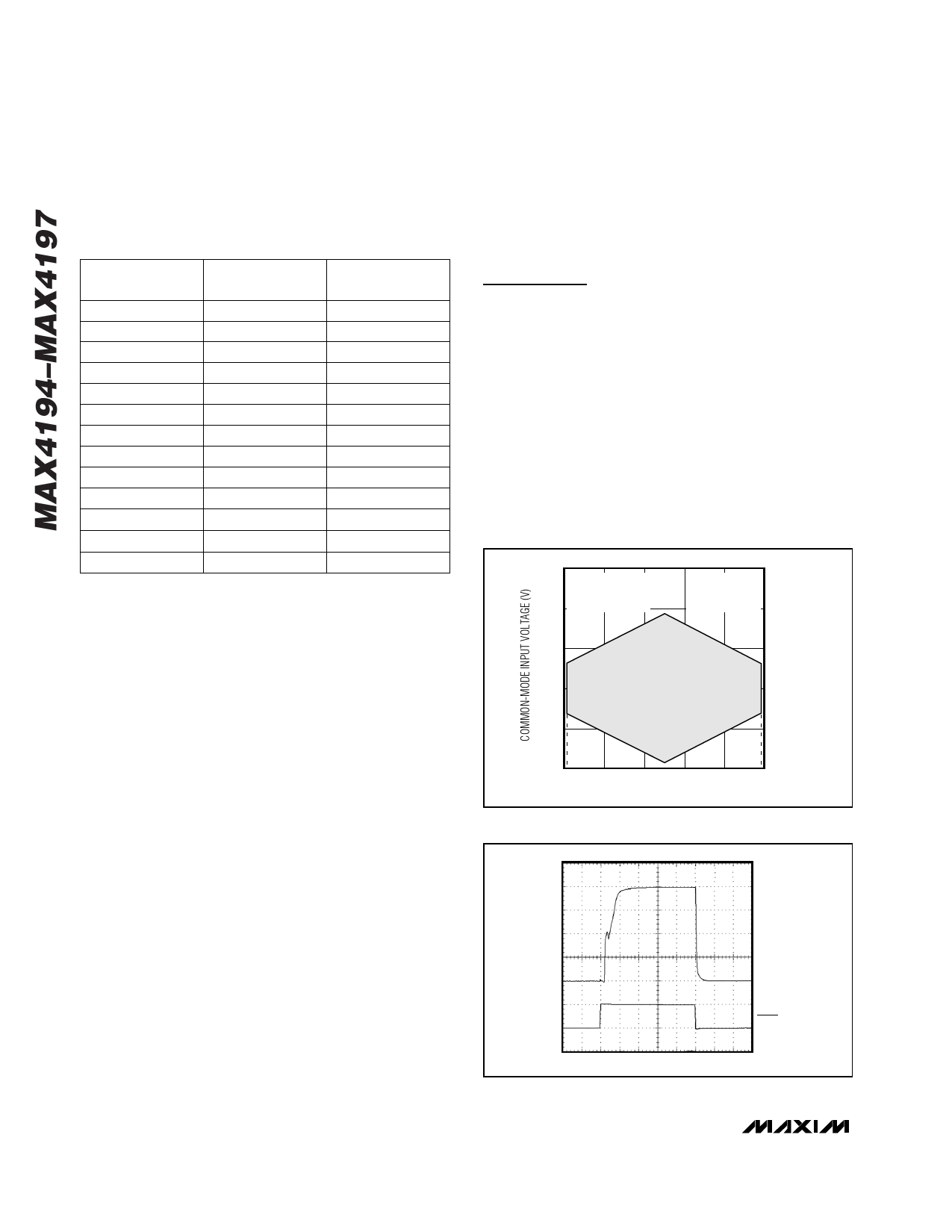
VCM vs. VOUT Characterization
Figure 4 illustrates the MAX4194 typical common-mode
input voltage range over output voltage swing at unity-
gain (pins 1 and 8 left floating), with a single-supply
voltage of VCC = +5V and a bias reference voltage of
VREF = VCC/2 = +2.5V. Points A and D show the full
input voltage range of the input amplifiers (VEE - 0.2V to
VCC - 1.1V) since, with +2.5V output, there is zero input
differential swing. The other points (B, C, E, and F) are
determined by the input voltage range of the input
amps minus the differential input amplitude necessary
to produce the associated VOUT. For the higher gain
configurations, the VCM range will increase at the end-
points (B, C, E, and F) since a smaller differential volt-
age is necessary for the given output voltage.
Rail-to-Rail Output Stage
The MAX4194–MAX4197’s output stage incorporates a
common-source structure that maximizes the dynamic
range of the instrumentation amplifier.
The output can drive up to a 25kΩ (tied to VCC/2) resis-
tive load and still typically swing within 30mV of the
rails. With an output load of 5kΩ tied to VCC/2, the out-
put voltage swings within 100mV of the rails.
Shutdown Mode
The MAX4195–MAX4197 feature a low-power shutdown
mode. When the shutdown pin (SHDN) is pulled low,
the internal amplifiers are switched off and the supply
current drops to 8µA typically (Figures 5a, 5b, and 5c).
This disables the instrumentation amplifier and puts its
output in a high-impedance state. Pulling SHDN high
enables the instrumentation amplifier.
Applications Information
Setting the Gain (MAX4194)
The MAX4194’s gain is set by connecting a single,
external gain resistor between the two RG pins (pin 1
and pin 8), and can be described as:
G = 1 + 50kΩ / RG
where G is the instrumentation amplifier’s gain and RG
is the gain-setting resistor.
The 50kΩ resistor of the gain equation is the sum of the
two resistors internally connected to the feedback loops
of the IN+ and IN- amplifiers. These embedded feed-
back resistors are laser trimmed, and their accuracy
and temperature coefficients are included in the gain
and drift specification for the MAX4194.
5
MAX4194/MAX4195
G = +1V/V
4 REF = +2.5V/+1.5V
A
VCC = +5V/+3V
VEE = 0
TA = +25°C
3
B
F
2
C
E
1
0.03
0
0
D
1
2
3
OUTPUT VOLTAGE (V)
4.97
4
5
Figure 4. Common-Mode Input Voltage vs. Output Voltage
MAX4195
OUT
AC-COUPLED
(VDIFF = 2V,
G = +1V/V)
(500mV/div)
50µs/div
Figure 5a. MAX4195 Shutdown Mode
SHDN
(5V/div)
10 ______________________________________________________________________________________
Share Link: