MAX4717(2002) 查看數據表(PDF) - Maxim Integrated
零件编号
产品描述 (功能)
生产厂家
MAX4717 Datasheet PDF : 15 Pages
| |||
4.5Ω/20Ω, 300MHz Bandwidth, Dual SPDT
Analog Switches in UCSP
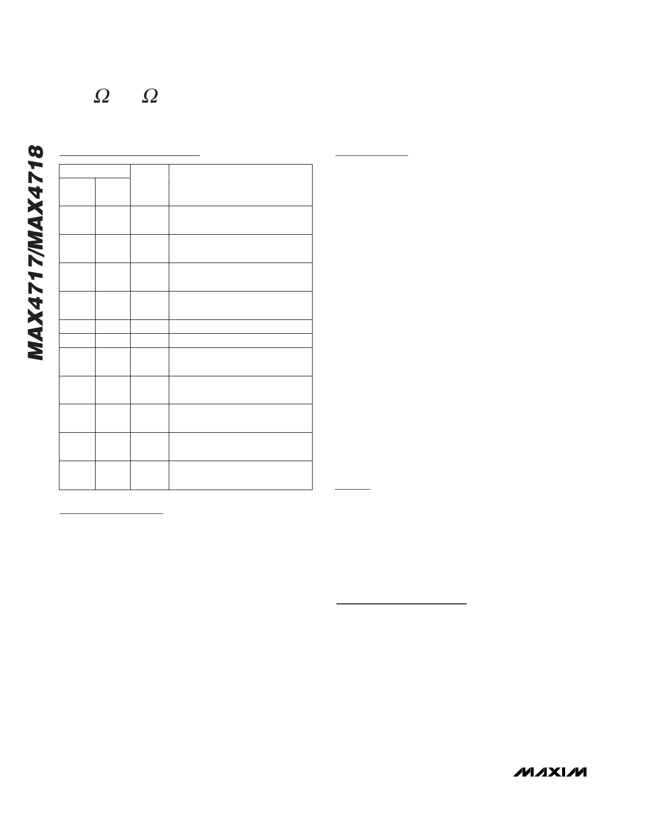
Pin Description
PIN
NAME
UCSP µMAX
FUNCTION
A1
7
NC2
Analog Switch 2—Normally Closed
Terminal
A2
8
IN2
Digital Control Input for Analog
Switch 2
A3
9
COM2
Analog Switch 2—Common
Terminal
A4
10
NO2
Analog Switch 2—Normally Open
Terminal
B1
6
GND Ground
B4
1
V+ Positive-Supply Voltage Input
C1
5
NC1
Analog Switch 1—Normally Closed
Terminal
C2
4
IN1
Digital Control Input for Analog
Switch 1
C3
3
COM1
Analog Switch 1—Common
Terminal
C4
2
NO1
Analog Switch 1—Normally Open
Terminal
Detailed Description
The MAX4717/MAX4718 high-speed, low-voltage, low on-
resistance (RON), dual SPDT analog switches operate
from a single +1.8V to +5.5V supply. The switches feature
break-before-make switching operation and fast switch-
ing speeds (tON = 80ns (max), tOFF = 40ns (max)).
These switches have low 15pF on-channel capaci-
tance, which allows for 12Mbps switching of the data
signals for USB 1.0/1.1 applications. The MAX4717 is
designed to switch D+ and D- USB signals with a guar-
anteed skew of less than 2ns (see Figure 4) as mea-
sured from 50% of the input signal to 50% of the output
signal.
Applications Information
Digital Control Inputs
The MAX4717/MAX4718 logic inputs accept up to
+5.5V regardless of supply voltage. For example, with
a +3.3V supply, IN_ can be driven low to GND and high
to +5.5V allowing for mixing of logic levels in a system.
Driving the control logic inputs rail-to-rail minimizes
power consumption. For a +3V supply voltage, the
logic thresholds are 0.5V (low) and 1.4V (high); for a
+5V supply voltage, the logic thresholds are 0.8V (low)
and 2.0V (high).
Analog Signal Levels
The on-resistance of the MAX4717/MAX4718 changes
very little for analog input signals across the entire supply
voltage range (see the Typical Operating Characteristics).
The switches are bidirectional, so the NO_, NC_, and
COM_ pins can be either inputs or outputs.
Power-Supply Sequencing and
Overvoltage Protection
Caution: Do not exceed the absolute maximum rat-
ings because stresses beyond the listed ratings
may cause permanent damage to the device.
Proper power-supply sequencing is recommended for
all CMOS devices. Always apply V+ before applying
analog signals, especially if the analog signal is not
current-limited.
UCSP Package Considerations
For general UCSP package information and PC layout
considerations, please refer to the Maxim Application
Note (Wafer-Level Chip-Scale Package).
UCSP Reliability
The chip-scale package (UCSP) represents a unique
packaging form factor that may not perform equally to a
packaged product through traditional mechanical relia-
bility tests. UCSP reliability is integrally linked to the
user’s assembly methods, circuit board material, and
usage environment. The user should closely review
these areas when considering use of a UCSP package.
Performance through Operating Life Test and Moisture
Resistance remains uncompromised as it is primarily
determined by the wafer-fabrication process.
Mechanical stress performance is a greater considera-
tion for a UCSP package. UCSPs are attached through
direct solder contact to the user’s PC board, foregoing
the inherent stress relief of a packaged product lead
frame. Solder joint contact integrity must be consid-
ered. Information on Maxim’s qualification plan, test
data, and recommendations are detailed in the UCSP
application note, which can be found on Maxim’s web-
site at www.maxim-ic.com.
Chip Information
TRANSISTOR COUNT: 235
PROCESS: BiCMOS
10 ______________________________________________________________________________________
Share Link: 