MAX6337US17D2-T жҹҘзңӢж•ёж“ҡиЎЁпјҲPDFпјү - Maxim Integrated
йӣ¶д»¶зј–еҸ·
дә§е“ҒжҸҸиҝ° (еҠҹиғҪ)
з”ҹдә§еҺӮ家
MAX6337US17D2-T
Maxim Integrated

MAX6337US17D2-T Datasheet PDF : 7 Pages
| |||
4-Pin, Ultra-Low-Voltage, Low-Power
ВөP Reset Circuits with Manual Reset
ABSOLUTE MAXIMUM RATINGS
Terminal Voltage (with respect to GND)
VCC ......................................................................-0.3V to +6V
Push/Pull RESET or RESET, MR ............-0.3V to (VCC + 0.3V)
Open-Drain RESET ..............................................-0.3V to +6V
Input Current (VCC) .............................................................20mA
Output Current (RESET, RESET).........................................20mA
Continuous Power Dissipation (TA = +70В°C)
SOT143 (derate 4mW/В°C above +70В°C) .....................320mW
Operating Temperature Range .........................-40В°C to +125В°C
Storage Temperature Range .............................-65В°C to +160В°C
Lead Temperature (soldering, 10s) .................................+300В°C
Stresses beyond those listed under вҖңAbsolute Maximum RatingsвҖқ may cause permanent damage to the device. These are stress ratings only, and functional
operation of the device at these or any other conditions beyond those indicated in the operational sections of the specifications is not implied. Exposure to
absolute maximum rating conditions for extended periods may affect device reliability.
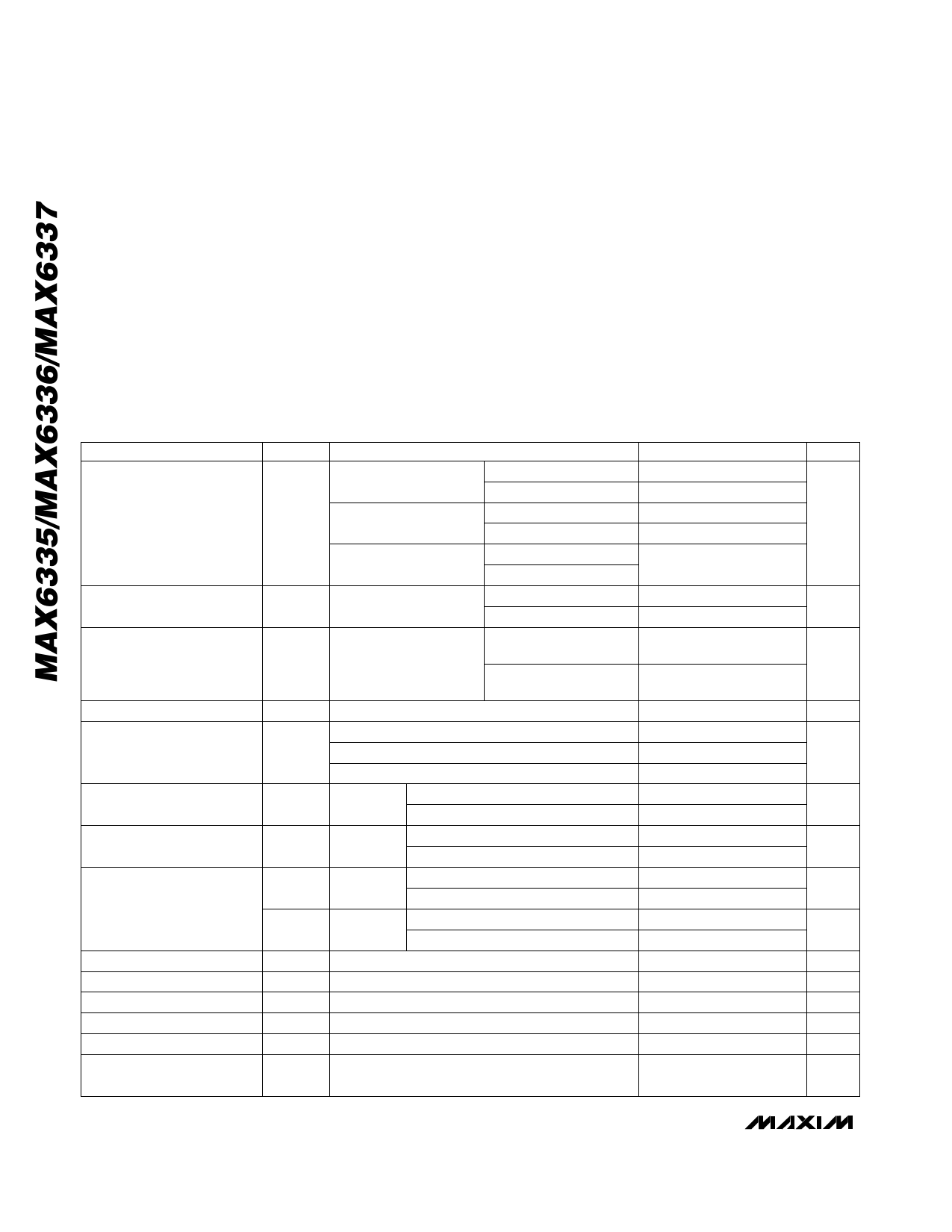
ELECTRICAL CHARACTERISTICS
(VCC = full range, MR = VCC or unconnected, TA = -40В°C to +125В°C, unless otherwise noted. Typical values are at TA = +25В°C and
VCC = 3V, reset not asserted.)
PARAMETER
Supply Voltage Range
Supply Current
SYMBOL
CONDITIONS
TA = 0В°C to +85В°C
MAX6335/MAX6336
MAX6337
VCC TA = -40В°C to +85В°C
MAX6335/MAX6336
MAX6337
TA = -40В°C to +125В°C
MAX6335/MAX6336
MAX6337
ICC No load
VCC = 1.8V
VCC = 2.5V
Reset Threshold
VTH
MAX633_US_ _D_-T,
Table 1
TA = +25В°C
TA = -40В°C to +125В°C
VCC Falling Reset Delay
Reset Active Timeout Period
RESET Output Low Voltage
(MAX6336/MAX6337)
RESET Output High Voltage
(MAX6336)
RESET Output Voltage
(MAX6335)
MR Minimum Pulse Width
MR Glitch Immunity
MR Reset Delay
MR Threshold
MR Pull-Up Resistance
RESET Output Leakage
Current (MAX6337)
VCC falling at 10V/ms
MAX633_US_ _D1-T
tRP MAX633_US_ _D2-T
MAX633_US_ _D3-T
VOL
Reset
asserted
ISINK = 50ВөA, VCC вүҘ 1.0V
ISINK = 500ВөA, VCC вүҘ 1.8V
VOH
VOH
Reset not
asserted
Reset
asserted
ISOURCE = 200ВөA, VCC вүҘ 1.8V
ISOURCE = 500ВөA, VCC вүҘ 2.7V
ISOURCE = 1ВөA, VCC вүҘ 1.0V
ISOURCE = 200ВөA, VCC вүҘ 1.8V
VOL
Reset not
asserted
ISINK = 500ВөA, VCC вүҘ 1.8V
ISINK = 1.2mA, VCC вүҘ 2.7V
V MR
VCC = 2.6V
VCC = 2.6V
VCC > VTH, RESET deasserted
MIN
0.7
1.0
0.78
1.2
1.2
VTH -
1.8%
VTH -
3%
1
20
100
0.8VCC
0.8VCC
0.8VCC
0.8VCC
1
0.3VCC
12
TYP
3.0
3.3
VTH
VTH
24
1.5
30
150
160
0.42
20
MAX
5.5
5.5
5.5
5.5
UNITS
V
5.5
6.0
ВөA
7.0
VTH +
1.8%
V
VTH +
3%
Вөs
2
40
ms
200
0.4
V
0.3
V
V
0.3
V
0.3
Вөs
ns
Вөs
0.7VCC V
30
kв„Ұ
0.5
ВөA
2 _______________________________________________________________________________________
Share Link: