MAX684 查看數據表(PDF) - Maxim Integrated
零件编号
产品描述 (功能)
生产厂家
MAX684 Datasheet PDF : 12 Pages
| |||
3.3V-Input to Regulated 5V-Output
Charge Pumps
Power Dissipation
The power dissipated in the MAX682/MAX683/MAX684
depends on output current and is accurately described
by:
PDISS = IOUT (2VIN - VOUT)
PDISS must be less than that allowed by the package
rating. See the Absolute Maximum Ratings for 8-pin
µMAX (MAX683/MAX684) and SO (MAX682) power-
dissipation limits and deratings.
Layout Considerations
All capacitors should be soldered in close proximity to
the IC. Connect ground and power ground through a
short, low-impedance trace. If a high-value resistor is
driving the shutdown input and is picking up noise (i.e.,
frequency jitter at CXP and CXN), bypass SHDN to
GND with a small capacitor (0.01µF).
Paralleling Devices
The MAX682/MAX683/MAX684 can be paralleled to
yield higher load currents. The circuit of Figure 6 can
deliver 500mA at 5V. It uses two MAX682s in parallel.
The devices can share the output capacitors, but each
one requires its own transfer capacitor (CX) and input
capacitor. For best performance, the paralleled devices
should operate in the same mode (skip or constant fre-
quency).
Chip Information
TRANSISTOR COUNT: 659
SUBSTRATE CONNECTED TO GND
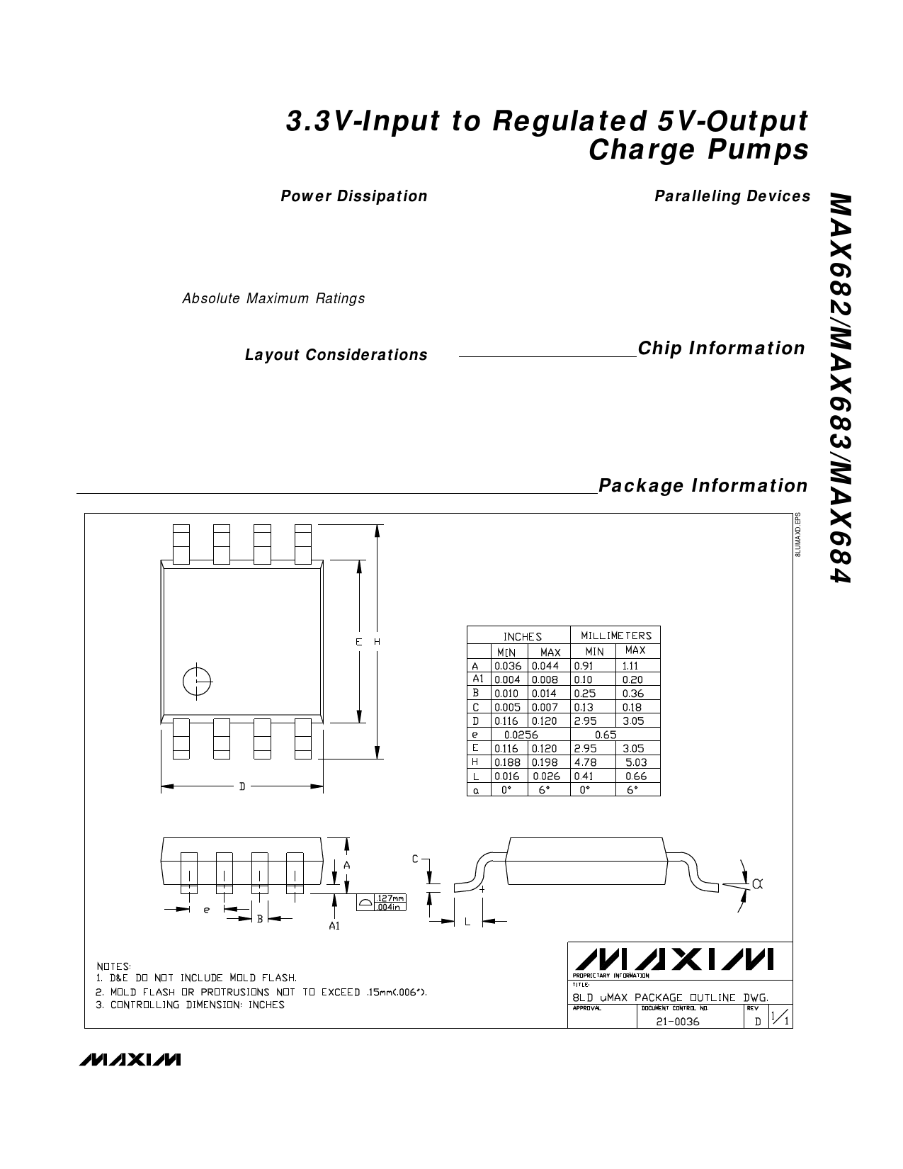
Package Information
_______________________________________________________________________________________ 9
Share Link: 