Q67100-H3509 жҹҘзңӢж•ёж“ҡиЎЁпјҲPDFпјү - Infineon Technologies
йӣ¶д»¶зј–еҸ·
дә§е“ҒжҸҸиҝ° (еҠҹиғҪ)
з”ҹдә§еҺӮ家
Q67100-H3509
Infineon Technologies

Q67100-H3509 Datasheet PDF : 27 Pages
| |||
SLx 24C08/16/P
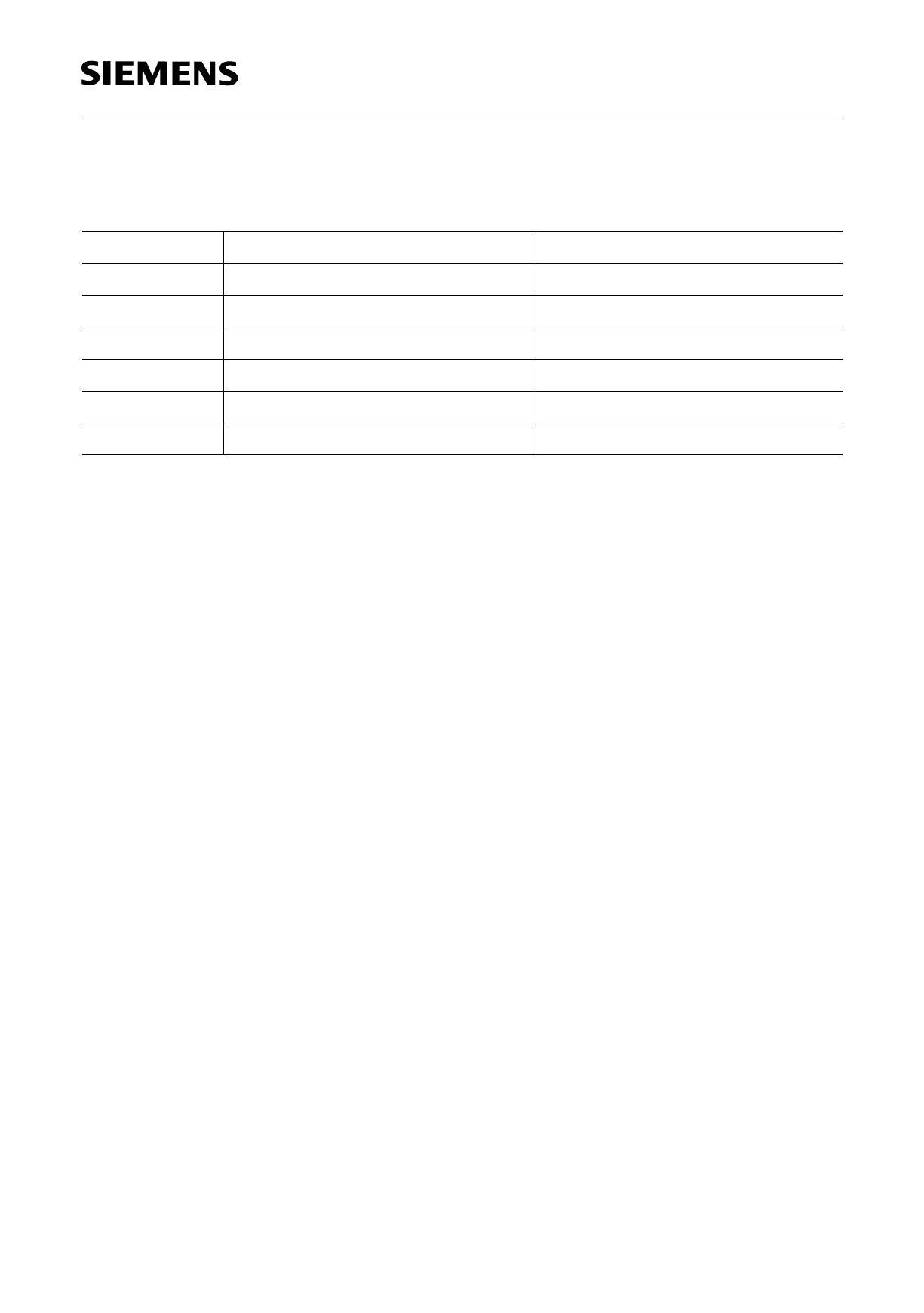
Pin Definitions and Functions
Table 1
Pin No.
Symbol
1, 2, 3
N.C.
4
VSS
5
SDA
6
SCL
7
WP
8
VCC
Function
Not connected
Ground
Serial bidirectional data bus
Serial clock input
Write protection input
Supply voltage
Pin Description
Serial Clock (SCL)
The SCL input is used to clock data into the device on the rising edge and to clock data
out of the device on the falling edge.
Serial Data (SDA)
SDA is a bidirectional pin used to transfer addresses, data or control information into the
device or to transfer data out of the device. The output is open drain, performing a wired
AND function with any number of other open drain or open collector devices. The SDA
bus requires a pull-up resistor to VCC.
Write Protection (WP)
WP switched to VSS allows normal read/write operations.
WP switched to VCC protects the entire EEPROM against changes (hardware write
protection).
Additionally write protection is managed by a protection bit associated to each page.
(refer to chapter 7 Page Protection ModeTM)
Semiconductor Group
5
1998-07-27
Share Link: