MAX6900 查看數據表(PDF) - Maxim Integrated
零件编号
产品描述 (功能)
生产厂家
MAX6900 Datasheet PDF : 17 Pages
| |||
I2C-Compatible RTC in a TDFN
DATA OUTPUT
BY TRANSMITTER
D7
D6
D0
DATA OUTPUT
BY RECEIVER
NOT ACKNOWLEDGE
ACKNOWLEDGE
CLK9
SCL FROM
MASTER
1
2
8
9
S
CLK1
CLK2
START
CONDITION
CLK8
CLOCK PULSE FOR
ACKNOWLEDGMENT
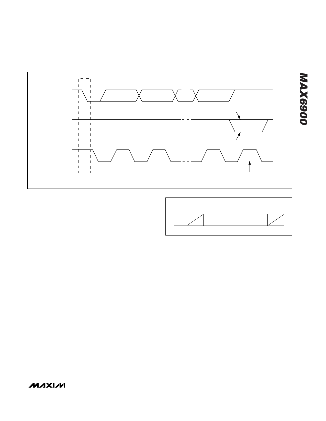
Figure 7. I2C Bus Acknowledge
An unlimited number of data bytes between the start
and stop conditions can be sent between the transmit-
ter and receiver. Each 8-bit byte is followed by an
acknowledge bit. Also, a master receiver must gener-
ate an acknowledge after each byte it receives that has
been clocked out of the slave transmitter.
The device that acknowledges must pull down the SDA
line during the acknowledge clock pulse (Figure 7), so
that the SDA line is stable low during the high period of
the acknowledge clock pulse (setup and hold times
must also be met). A master receiver must signal an
end of data to the transmitter by not generating an
acknowledge on the last byte that has been clocked
out of the slave. In this case, the transmitter must leave
SDA high to enable the master to generate a stop con-
dition. Any time a stop condition is received before the
current byte of data transfer is complete, the last incom-
plete byte is ignored.
The second byte of data sent after the start condition is
the Address/Command byte (Figure 8). Each data
transfer is initiated by an Address/Command byte. The
MSB (bit 7) must be a logic 1. When the MSB is zero,
Writes to the MAX6900 are disabled. Bit 6 specifies
clock/calendar data if logic 0 or RAM data if logic 1
(Tables 1 and 2). Bits 1 through 5 specify the designat-
ed registers to be input or output. The LSB (bit 0) spec-
ifies a Write operation (input) if logic 0 or Read
operation (output) if logic 1. The Command byte is
always input starting with the MSB (bit 7).
A7
A6
A5 A4 A3 A2 A1
A0
RAM
1
A5
A4
A3
A2
A1 RD
/CLK
/W
Figure 8. Address/Command Byte
Reading from the Timekeeping
Registers
The timekeeping registers (Seconds, Minutes, Hours,
Date, Month, Day, Year, and Century) read either with a
Single Read or a Burst Read. Since the clock runs con-
tinuously and a Read takes a finite amount of time, it is
possible that the clock counters could change during a
Read operation, thereby reporting inaccurate timekeep-
ing data. In the MAX6900, the clock counter data is
buffered by a latch. Clock counter data is latched by the
I2C-bus-compatible read command (on the falling edge
of SCL when the Slave Acknowledge bit is sent after the
Address/Command byte has been sent by the master to
read a timekeeping register). Collision-detection circuitry
ensures that this does not happen coincident with a sec-
onds counter update to ensure accurate time data is
being read. This avoids time data changes during a
Read operation. The clock counters continue to count
and keep accurate time during the Read operation.
When using a Single Read to read each of the time-
keeping registers individually, perform error checking
_______________________________________________________________________________________ 7
Share Link: 