MAX6901 查看數據表(PDF) - Maxim Integrated
零件编号
产品描述 (功能)
生产厂家
MAX6901 Datasheet PDF : 18 Pages
| |||
3-Wire Serial RTC in a TDFN
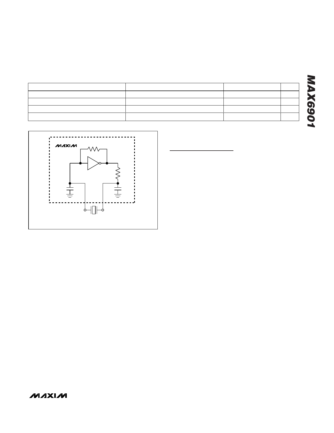
Table 1. Acceptable Quartz Crystal Parameters
PARAMETER
Frequency
Equivalent Series Resistance (ESR)
Parallel Load Capacitance
Q Factor
SYMBOL
f
Rs
CL
Q
MIN
40
11.2
40,000
TYP
32.76
12.5
MAX
60
13.7
60,000
UNITS
kHz
kΩ
pF
Rf
MAX6901
Cg
25pF
Rd
Cd
25pF
X1
X2
EXTERNAL
CRYSTAL
Figure 1. Oscillator Circuit Schematic
Clock Burst Mode
Accessing the Clock Burst register specifies burst-
mode operation. In this mode, multiple bytes are read
or written with a single Address/Command write. If the
Clock Burst register is accessed (BEh for Write and
BFh for Read), the first seven clock/calendar registers
(Seconds, Minutes, Hours, Date, Month, Day, and Year)
and the Control register, are consecutively read or writ-
ten, starting with the LSB of the Seconds register. When
writing to the clock registers in burst mode, all seven
registers must be written in order for the data to be
transferred (see Example: Setting the Clock with a
Burst Write).
RAM Burst Mode
Sending the RAM Burst Address/Command specifies
Burst-Mode operation. In this mode, the 31 RAM regis-
ters can be consecutively read or written, starting with
bit 0 of address C0h for Writes, and C1h for Reads.
Burst Read outputs all 31 registers of RAM. When writ-
ing to RAM in burst mode, it is not necessary to write all
31 bytes for the data to transfer; each complete byte
written is transferred to RAM. When reading from RAM,
data bits are output until all 31 bytes have been read,
or until CS is driven low.
Setting the Clock
Writing to the Timekeeping Registers
The Time and Date are set by writing to the timekeep-
ing registers (Seconds, Minutes, Hours, Date, Month,
Day, Year, and Century). During a write operation, an
input buffer accepts the new time data while the time-
keeping registers continue to increment normally,
based on the crystal counter. The buffer also keeps the
timekeeping registers from changing as the result of an
incomplete Write operation, and collision detection cir-
cuitry ensures that a time write does not occur coinci-
dent with a Seconds register increment. The updated
time data are loaded into the timekeeping registers on
the falling edge of CS, at the end of the 3-wire serial
Write operation. An incomplete Write operation aborts
the update procedure, and the contents of the input
buffer are discarded. The timekeeping registers reflect
the new time, beginning with the first Seconds register
increment after the falling edge of CS.
Although both Single Writes and Burst Writes are possi-
ble, the best way to write to the timekeeping registers is
with a Burst Write. With a Burst Write, main timekeeping
registers (Seconds, Minutes, Hours, Date, Month, Day,
Year), and the Control register are written sequentially
following the Address/Command byte. They must be
written as a group of eight registers, with 8 bits each,
for proper execution of the Burst Write function. All
seven timekeeping registers are simultaneously loaded
into the clock counters by the falling edge of CS, at the
end of the 3-wire serial Write operation. For a normal
burst data transfer, the worst-case error that can occur
between the actual time and the written time update is
1 second.
If Single Write operations are used to enter data into the
timekeeping registers, error checking is required. If the
Seconds register is not to be written, then begin by
reading the Seconds register and save it as initial-sec-
onds. Write to the required timekeeping registers and
_______________________________________________________________________________________ 5
Share Link: 