MAX6973 查看數據表(PDF) - Maxim Integrated
零件编号
产品描述 (功能)
生产厂家
MAX6973 Datasheet PDF : 23 Pages
| |||
16-Output PWM LED Drivers
for Message Boards
ABSOLUTE MAXIMUM RATINGS
(All voltages with respect to GND.)
VDD ........................................................................-0.3V to +4.0V
Y0–Y7, Z0–Z7, MUX0, and MUX1 .........................-0.3V to +8.0V
All Other Pins..............................................-0.3V to (VDD + 0.3V)
Continuous Power Dissipation (TA = +70°C)
32-Pin TQFN (derate 34.5mW/°C over +70°C) ..........2857mW
Operating Temperature Range .........................-40°C to +125°C
Junction Temperature ......................................................+150°C
Storage Temperature Range .............................-65°C to +150°C
Lead Temperature (soldering, 10s) .................................+300°C
Stresses beyond those listed under “Absolute Maximum Ratings” may cause permanent damage to the device. These are stress ratings only, and functional
operation of the device at these or any other conditions beyond those indicated in the operational sections of the specifications is not implied. Exposure to
absolute maximum rating conditions for extended periods may affect device reliability.
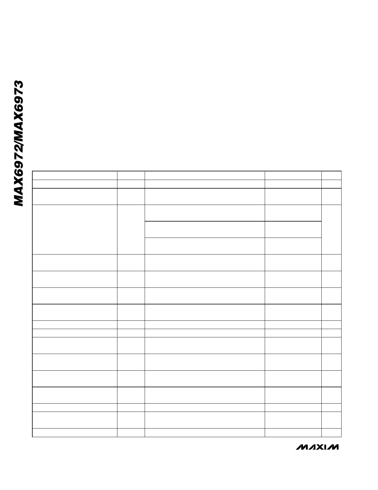
ELECTRICAL CHARACTERISTICS
(VDD = 3.0V to 3.6V, TA = TMIN to TMAX, unless otherwise noted. Typical values are at VDD = 3.3V, TA = +85°C.) (Note 1)
PARAMETER
SYMBOL
Operating Supply Voltage
VDD
LEDs Anode Voltage
(Y0–Y7, Z0–Z7, MUX0, and MUX1)
VO
CONDITIONS
MIN TYP MAX UNITS
3.0
3.6
V
7
V
fCLKI = 0Hz; CLKO_, DOUT_ loaded 200Ω;
calibration DACs set to 0x01
21 35
Supply Current
IDD
fCLKI = 0Hz; CLKO_, DOUT_ loaded 200Ω;
calibration DACs set to 0xFF
40 55 mA
fCLKI = 32MHz; CLKO_, DOUT_ loaded 200Ω;
calibration DACs set to 0xFF
42 60
Input High Voltage LOADI
VIHC
0.7
x VDD
V
Input Low Voltage LOADI
VILC
0.3
x VDD
V
Differential Input Voltage Range
CLKI_, DIN_
VID
±0.15
±1.20 V
Common-Mode Input Voltage
CLKI_, DIN_
Differential Input High Threshold
Differential Input Low Threshold
Differential Output Voltage
CLKO_, DOUT_
VCM
VDIFFTH
VDIFFTL
VOD Termination 200Ω at receiver _+ and _- inputs
|VID / 2|
2.4
V
8
65 mV
-65 -8
mV
±190
±550 mV
Differential Output Offset
CLKO_, DOUT_
VOS Termination 200Ω at receiver _+ and _- inputs
1.125 1.25 1.375 V
Input Leakage Current
CLKI_, DIN_, LOADI
IIH, IIL
-1
+1
µA
Input Capacitance
CLKI_, DIN_, LOADI
Output Low Voltage LOADO
Output High Voltage LOADO
Output Slew Time LOADO
VOLC
VOHC
ISINK = 5mA
ISOURCE = 5mA
20% to 80%, 80% to 20%, load = 10pF
10
pF
0.05 0.25
V
VDD
VDD
V
- 0.5 - 0.2
3
ns
2 _______________________________________________________________________________________
Share Link: 