MAX8862R 查看數據表(PDF) - Maxim Integrated
零件编号
产品描述 (功能)
生产厂家
MAX8862R Datasheet PDF : 12 Pages
| |||
Low-Cost, Low-Dropout, Dual Linear Regulator
100
80
60
40
20
0
0 5 10 15 20 25 30 35
PC-BOARD COPPER FOIL AREA (Cm2)
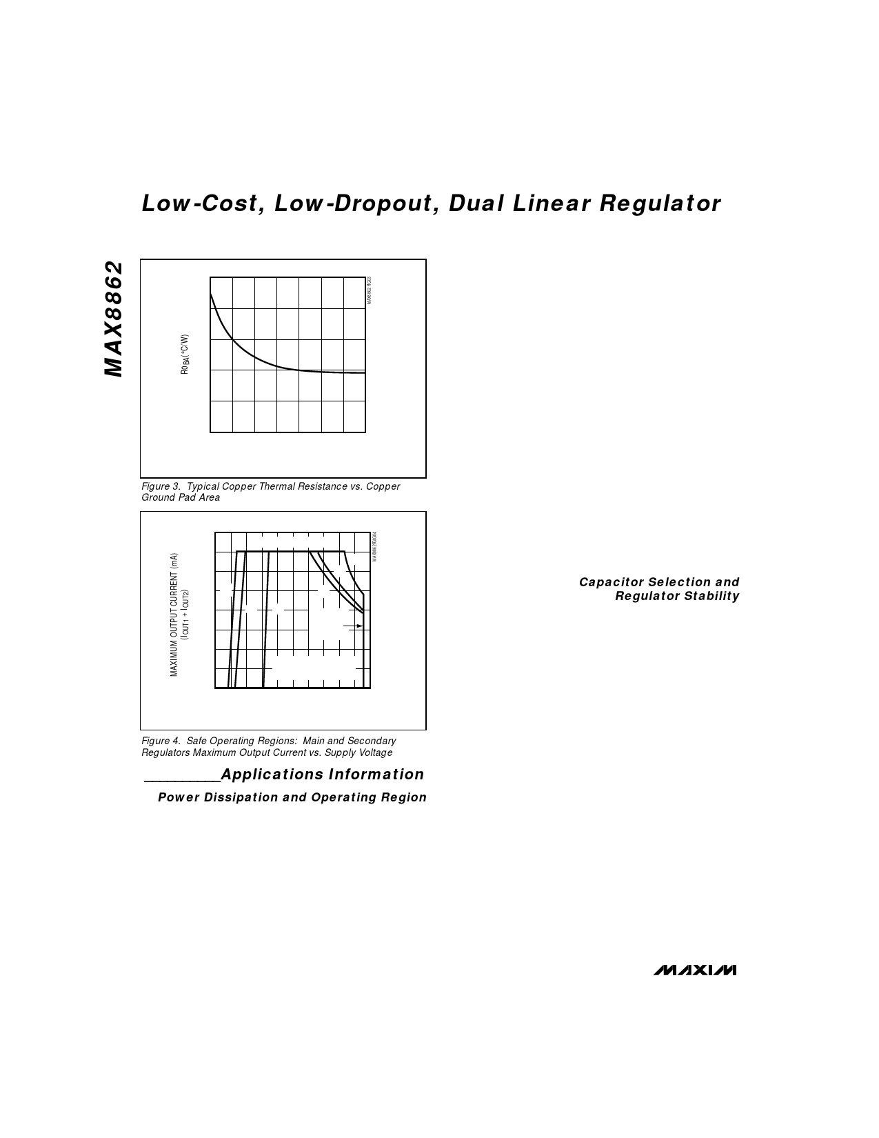
Figure 3. Typical Copper Thermal Resistance vs. Copper
Ground Pad Area
400
MAXIMUM CURRENT
350
(L)
300
(T)
250 (R)
(R)
200
(T) (L)
MAXIMUM
150
SUPPLY
VOLTAGE
100
OPERATING REGION AT
50
TA = +25°C, TJ = +125°C
0
2 3 4 5 6 7 8 9 10 11 12
SUPPLY VOLTAGE (V)
Figure 4. Safe Operating Regions: Main and Secondary
Regulators Maximum Output Current vs. Supply Voltage
__________Applications Information
Power Dissipation and Operating Region
The MAX8862’s maximum power dissipation depends
on the thermal resistance of the case and circuit board,
the temperature difference between the die junction
and ambient air, and the rate of air flow.
The GND pins of the MAX8862 SO package perform
the dual function of providing an electrical connection
to ground and channeling heat away. Connect all GND
pins to ground using a large pad or ground plane.
Where this is impossible, place a copper plane on an
adjacent layer. For a given power dissipation, the pad
should exceed the associated dimensions in Figure 3.
This figure shows a typical thermal resistance for a
35µm-thick copper foil as a function of its area1.
The power dissipation across the device is given by:
P = IOUT1 (VIN1 - VOUT1) + IOUT2 (VIN2 - VOUT2).
The resulting power dissipation is as follows:
P = (TJ - TA) / (θJB + θBA)
where (TJ - TA) is the temperature difference between
the MAX8862 die junction and the surrounding air, θJB
(or θJC) is the thermal resistance of the package, and
θBA is the thermal resistance through the printed circuit
board, copper traces, and other materials to the sur-
rounding air. The MAX8862’s narrow SO package has a
thermal resistance of θJB = +50°C/W.
The MAX8862 regulators deliver the rated output cur-
rents and operate with input voltages up to 11.5V, but
not simultaneously. High output currents can only be
sustained when input-output differential voltages are
small, as shown in Figure 4.
Capacitor Selection and
Regulator Stability
Filter capacitors are required at the MAX8862’s inputs
and outputs. 1µF ceramic capacitors are required at
the inputs. The minimum output capacitance required
for stability is 3.3µF for OUT1 and 2.2µF for OUT2. The
capacitor values depend primarily on the desired
power-up time and load-transient response. Load-
transient response is improved by using larger capaci-
tor values. Input and output filter capacitors should be
soldered directly to pins to minimize lead inductance of
PC board traces.
The output capacitor’s equivalent series resistance
(ESR) affects stability and output noise. Surface-mount
ceramic capacitors have a very low ESR and are avail-
able up to 10µF. Otherwise, other low-ESR (<0.5Ω)
capacitors should be used. If the selected capacitor’s
ESR is higher than the recommended value, the capac-
itor value should be increased proportionally to main-
tain minimum output noise under all input voltage and
output load conditions. Paralleling two or more capaci-
tors also results in lower ESR.
1This graph was generated by Mr. Kieran O’Malley of Cherry Semiconductor Corp. and was published in the October 26, 1995, issue
of EDN magazine.
10 ______________________________________________________________________________________
Share Link: 