MAX8862 查看數據表(PDF) - Maxim Integrated
零件编号
产品描述 (功能)
生产厂家
MAX8862 Datasheet PDF : 12 Pages
| |||
Low-Cost, Low-Dropout, Dual Linear Regulator
MAX8862
OUT_
SET_
GND
OUTPUT
R1
R2
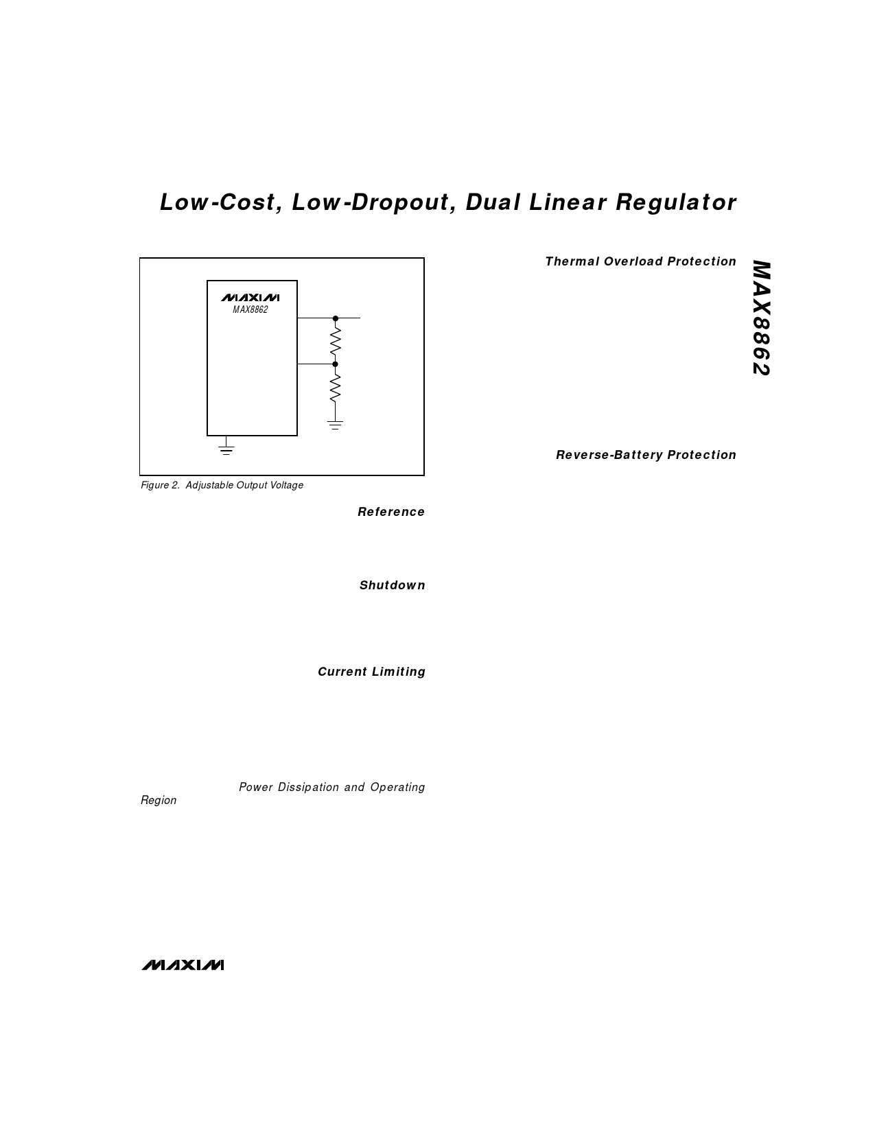
Figure 2. Adjustable Output Voltage
Reference
The MAX8862 provides a precision 1.25V reference at
REF2. Bypass REF2 with a 0.1µF capacitor to ground.
Larger bypassing capacitors will further reduce the
secondary regulator’s wideband noise.
Shutdown
The MAX8862’s regulators have individual shutdown
controls. A logic low on either SHDN1 or SHDN2 turns
off the corresponding internal reference, error com-
parator, and pass transistors’ control logic, reducing
quiescent current to less than 1µA.
Current Limiting
The MAX8862 features a current limit for each regula-
tor. It monitors and controls the pass transistor’s gate
voltage, limiting the output current to 580mA for the
main regulator and 250mA for the secondary regulator.
The current limits apply to all input and output voltage
conditions. The outputs can be shorted to ground for
an indefinite period of time if the package can dissipate
(VIN1 x ILIM1 + VIN2 x ILIM2) without exceeding TJ =
+150°C (see the Power Dissipation and Operating
Region section).
Thermal Overload Protection
Thermal overload protection limits the MAX8862’s total
power dissipation. When the junction temperature
exceeds TJ = +160°C, the thermal sensor sends a sig-
nal to the shutdown logic, turning off the pass transis-
tors and allowing the device to cool down. The thermal
sensor turns the pass transistors on again after the IC’s
junction temperature decreases by 20°C. If the thermal
overload condition persists, OUT1 and OUT2 pulse on
and off.
Thermal overload protection is designed to protect the
MAX8862 during fault conditions. For continuous oper-
ation, the absolute maximum junction temperature rat-
ing of TJ = +150°C should not be exceeded.
Reverse-Battery Protection
This feature protects the MAX8862 against polarity
reversal at the supply inputs. The inputs can handle
negative voltages up to -12V without suffering any ill
effects. When the input polarity is reversed, the output
will be at the same potential as ground, and no current
will flow from the output back to the input. This feature
protects both the device and the supply-voltage
source. The reverse currents that flow back to the input
are due to RPWROK1 , RSHDN1, and RSHDN2. These
currents are approximately: IREV1 = |VIN1| / (RSHDN1 +
RPWROK1) and IREV2 = |VIN2| / RSHDN2. When operat-
ing the MAX8862 in continuous mode (VSHDN1 = VIN1
and VSHDN2 = VIN2) place a resistor (>20kΩ) between
shutdown and supply inputs to limit the current flow in
case the battery is reversed.
_______________________________________________________________________________________ 9
Share Link: 