MAX8740 查看數據表(PDF) - Maxim Integrated
零件编号
产品描述 (功能)
生产厂家
MAX8740 Datasheet PDF : 12 Pages
| |||
TFT-LCD Step-Up DC-DC Converter
V2
+28V C9
1µF
C7 C8
D3
D2 0.1µF 0.1µF
V3
-10V
C10
0.22µF
VIN
4.5V TO 5.5V
C1
10µF
R4
6.3V
10Ω
C5
1µF
L1
2.7µH
D1
6
LX
8
IN
7
LX
FB 2
9
FREQ
3 SHDN
MAX8740
GND 5
GND 4
C2
C7
R1
10µF
10µF
196kΩ
25V
25V
1%
R2
20kΩ
1%
10
SS
C4
33nF
COMP 1
R3
47kΩ
1%
C6
68pF
C3
560pF
VOUT
13.5V/800mA
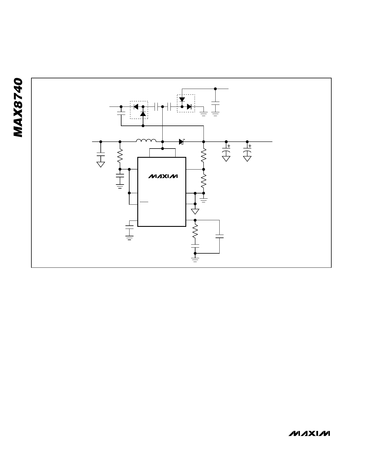
Figure 3. Multiple-Output TFT-LCD Power Supply
Multiple-Output Power Supply for TFT LCD
Figure 3 shows a power supply for active-matrix TFT-
LCD flat-panel displays. Output-voltage transient perfor-
mance is a function of the load characteristic. Add or
remove output capacitance (and recalculate compensa-
tion-network component values) as necessary to meet
the required transient performance. Regulation perfor-
mance for secondary outputs (V2 and V3) depends on
the load characteristics of all three outputs.
PC Board Layout and Grounding
Careful PC board layout is important for proper operation.
Use the following guidelines for good PC board layout:
1) Minimize the area of high-current loops by placing
the inductor, rectifier diode, and output capacitors
near the input capacitors and near the LX and GND
pins. The high-current input loop goes from the
positive terminal of the input capacitor to the induc-
tor, to the IC’s LX pin, out of GND, and to the input
capacitor’s negative terminal. The high-current out-
put loop is from the positive terminal of the input
capacitor to the inductor, to the rectifier diode (D1),
and to the positive terminal of the output capacitors,
reconnecting between the output capacitor and
input capacitor ground terminals. Connect these
loop components with short, wide connections.
Avoid using vias in the high-current paths. If vias
are unavoidable, use many vias in parallel to
reduce resistance and inductance.
2) Create a power ground island (PGND) consisting of
the input and output capacitor grounds and GND
pins. Connect all of these together with short, wide
traces or a small ground plane. Maximizing the
width of the power ground traces improves efficien-
cy and reduces output voltage ripple and noise
spikes. Create an analog ground plane (AGND)
consisting of the feedback-divider ground connec-
tion, the COMP and SS capacitor ground connec-
tions, and the device’s exposed backside pad.
Connect the AGND and PGND islands by connect-
ing the GND pins directly to the exposed backside
pad. Make no other connections between these
separate ground planes.
10 ______________________________________________________________________________________
Share Link: 