MAX8740 查看數據表(PDF) - Maxim Integrated
零件编号
产品描述 (功能)
生产厂家
MAX8740 Datasheet PDF : 12 Pages
| |||
TFT-LCD Step-Up DC-DC Converter
Pin Description
PIN NAME
FUNCTION
1
COMP Compensation Pin for Error Amplifier. Connect a series RC from COMP to ground. See the Loop
Compensation section for component selection guidelines.
Feedback Pin. The FB regulation voltage is 1.24V nominal. Connect an external resistive voltage-divider
2
FB
between the step-up regulator’s output (VOUT) and GND, with the center tap connected to FB. Place the
divider close to the IC and minimize the trace area to reduce noise coupling. Set VOUT according to the
Output Voltage Selection section.
3
SHDN Shutdown Control Input. Drive SHDN low to turn off the MAX8740.
4, 5
GND Ground. Connect pins 4 and 5 directly together.
6, 7
LX
Switch Pin. LX is the drain of the internal MOSFET. Connect the inductor/rectifier diode junction to LX and
minimize the trace area for lower EMI. Connect pins 6 and 7 directly together.
8
IN Supply Pin. Bypass IN with a minimum 1µF ceramic capacitor directly to GND.
9
FREQ
Frequency-Select Input. When FREQ is low, the oscillator frequency is set to 640kHz. When FREQ is high, the
frequency is 1.2MHz. This input has a 5µA pulldown current.
Soft-Start Control Pin. Connect a soft-start capacitor (CSS) to this pin. Leave open for no soft-start. The soft-
10
SS
start capacitor is charged with a constant current of 4.5µA. Full current limit is reached after t = 2.5 x 10⁵ CSS.
The soft-start capacitor is discharged to ground when SHDN is low. When SHDN goes high, the soft-start
capacitor is charged to 0.4V, after which soft-start begins.
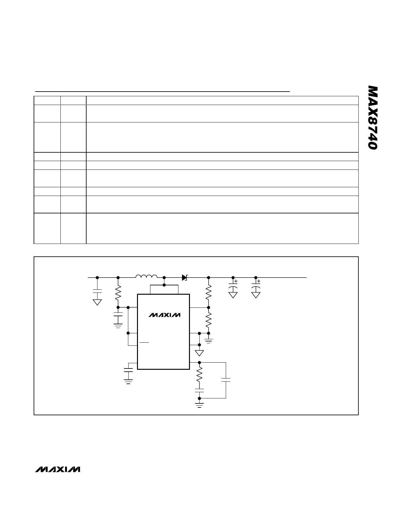
VIN
4.5V TO 5.5V
C1
10µF
R3
6.3V
10Ω
C3
1µF
L1
2.7µH
D1
6
LX
8
IN
7
LX
FB 2
9
FREQ
3 SHDN
MAX8740
GND 5
GND 4
C2
C7
R1
10µF
10µF
196kΩ
20V
20V
1%
R2
20kΩ
1%
10 SS
C6
33nF
COMP 1
R4
47kΩ
1%
C5
68pF
C4
560pF
VOUT
13.5V/800mA
Figure 1. Typical Operating Circuit
_______________________________________________________________________________________ 5
Share Link: 