MC14562B 查看數據表(PDF) - ON Semiconductor
零件编号
产品描述 (功能)
生产厂家
MC14562B Datasheet PDF : 8 Pages
| |||
MC14562B
128-Bit Static Shift
Register
The MC14562B is a 128–bit static shift register constructed with
MOS P–channel and N–channel enhancement mode devices in a
single monolithic structure. Data is clocked in and out of the shift
register on the positive edge of the clock input. Data outputs are
available every 16 bits, from 16 through bit 128. This complementary
MOS shift register is primarily used where low power dissipation
and/or high noise immunity is desired.
• Diode Protection on All Inputs
• Fully Static Operation
• Cascadable to Provide Longer Shift Register Lengths
• Supply Voltage Range = 3.0 Vdc to 18 Vdc
• Capable of Driving Two Low–power TTL Loads or One Low–power
Schottky TTL Load Over the Rated Temperature Range
MAXIMUM RATINGS (Voltages Referenced to VSS) (Note 1.)
Symbol
Parameter
Value
Unit
VDD
DC Supply Voltage Range
– 0.5 to +18.0
V
Vin, Vout Input or Output Voltage Range – 0.5 to VDD + 0.5
V
(DC or Transient)
Iin, Iout
Input or Output Current
(DC or Transient) per Pin
± 10
mA
PD
Power Dissipation,
per Package (Note 2.)
500
mW
TA
Ambient Temperature Range
Tstg
Storage Temperature Range
TL
Lead Temperature
(8–Second Soldering)
– 55 to +125
°C
– 65 to +150
°C
260
°C
1. Maximum Ratings are those values beyond which damage to the device
may occur.
2. Temperature Derating:
Plastic “P and D/DW” Packages: – 7.0 mW/_C From 65_C To 125_C
This device contains protection circuitry to guard against damage due to high
static voltages or electric fields. However, precautions must be taken to avoid
applications of any voltage higher than maximum rated voltages to this
v v high–impedance circuit. For proper operation, Vin and Vout should be constrained
to the range VSS (Vin or Vout) VDD.
Unused inputs must always be tied to an appropriate logic voltage level (e.g.,
either VSS or VDD). Unused outputs must be left open.
http://onsemi.com
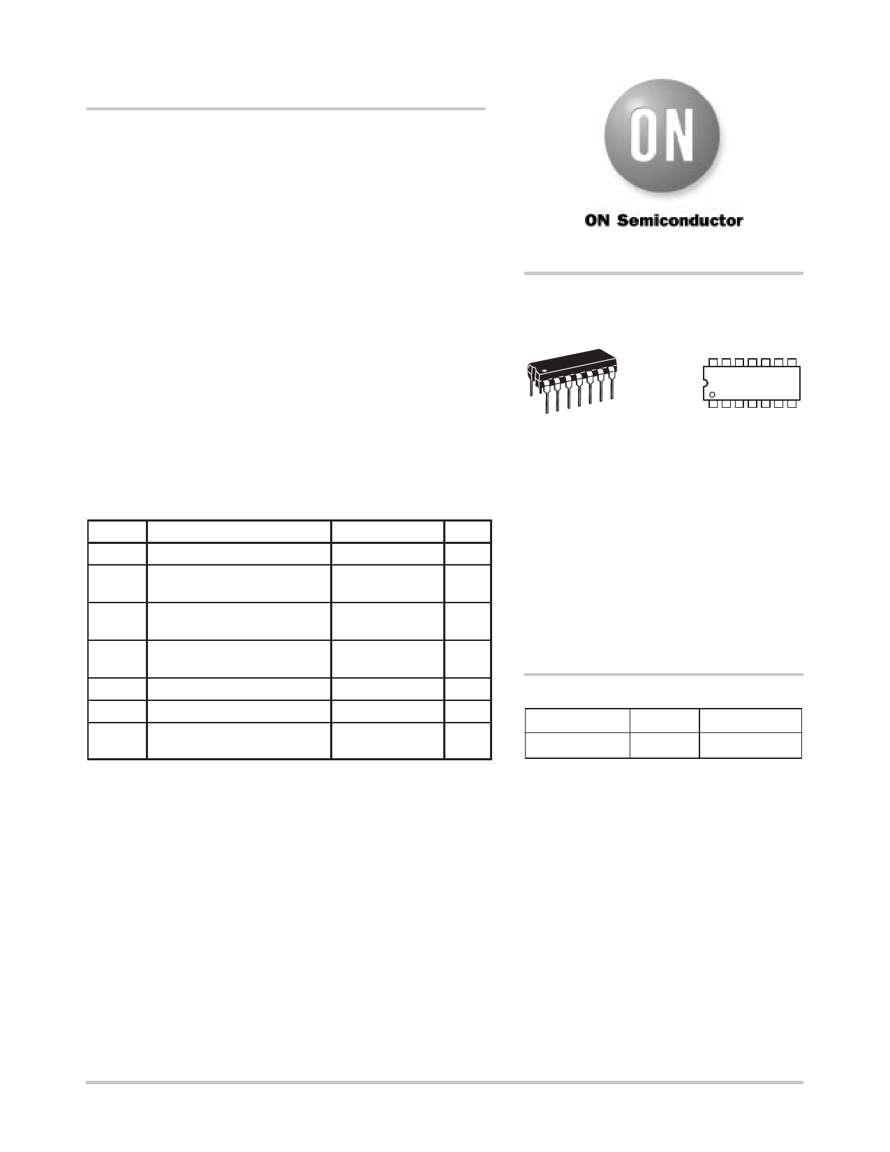
PDIP–14
P SUFFIX
CASE 646
MARKING
DIAGRAMS
14
MC14562BCP
AWLYYWW
1
A
= Assembly Location
WL or L = Wafer Lot
YY or Y = Year
WW or W = Work Week
ORDERING INFORMATION
Device
Package
Shipping
MC14562BCP
PDIP–14
25/Rail
© Semiconductor Components Industries, LLC, 2000
1
March, 2000 – Rev. 3
Publication Order Number:
MC14562B/D
Share Link: 