MC74HC125A 查看數據表(PDF) - ON Semiconductor
零件编号
产品描述 (功能)
生产厂家
MC74HC125A Datasheet PDF : 8 Pages
| |||
MC74HC125A, MC74HC126A
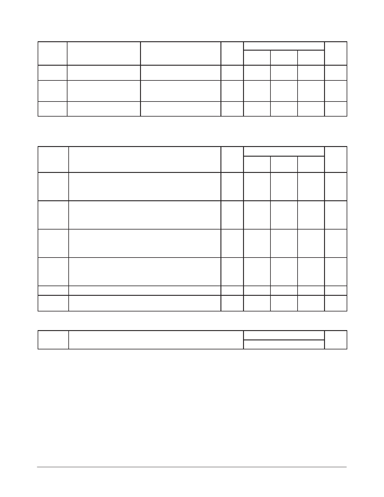
DC ELECTRICAL CHARACTERISTICS (Voltages Referenced to GND)
ÎÎÎÎÎÎÎÎÎÎÎÎÎÎÎÎÎÎÎÎÎÎÎÎÎÎÎÎÎÎÎÎÎ Guaranteed Limit
ÎÎÎÎÎÎÎÎÎÎÎÎÎÎÎÎÎÎÎÎÎÎÎÎÎÎÎÎÎÎÎÎÎ Symbol
Parameter
Test Conditions
VCC
V
– 55 to
25_C
v v 85_C
125_C Unit
ÎÎÎÎÎÎÎÎÎÎÎÎÎÎÎÎÎÎÎÎÎÎÎÎÎÎÎÎÎÎÎÎÎ Iin
Maximum Input Leakage
ÎÎÎÎÎÎÎÎÎÎÎÎÎÎÎÎÎÎÎÎÎÎÎÎÎÎÎÎÎÎÎÎÎ Current
Vin = VCC or GND
6.0
± 0.1
± 1.0
± 1.0
µA
ÎÎÎÎÎÎÎÎÎÎÎÎÎÎÎÎÎÎÎÎÎÎÎÎÎÎÎÎÎÎÎÎÎ IOZ
Maximum Three–State
ÎÎÎÎÎÎÎÎÎÎÎÎÎÎÎÎÎÎÎÎÎÎÎÎÎÎÎÎÎÎÎÎÎ Leakage Current
Output in High–Impedance State
6.0
± 0.5
± 5.0
± 10
µA
Vin = VIL or VIH
Vout = VCC or GND
ÎÎÎÎÎÎÎÎÎÎÎÎÎÎÎÎÎÎÎÎÎÎÎÎÎÎÎÎÎÎÎÎÎ ICC
Maximum Quiescent Supply Vin = VCC or GND
Current (per Package)
Iout = 0 µA
6.0
4.0
40
160
µA
ÎÎÎÎÎÎÎÎÎÎÎÎÎÎÎÎÎÎÎÎÎÎÎÎÎÎÎÎÎÎÎÎÎÎÎÎÎÎÎÎÎÎÎÎÎÎÎÎÎÎÎÎÎÎÎÎÎÎÎÎÎÎÎÎÎÎ NOTE:Information on typical parametric values can be found in Chapter 2 of the ON Semiconductor High–Speed CMOS Data Book
(DL129/D).
AC ELECTRICAL CHARACTERISTICS (CL = 50 pF, Input tr = tf = 6.0 ns)
Guaranteed Limit
ÎÎÎÎÎÎÎÎÎÎÎÎÎÎÎÎÎÎÎÎÎÎÎÎÎÎÎÎÎÎÎÎÎÎÎÎÎÎÎÎÎÎÎÎÎÎÎÎÎÎÎÎÎÎÎÎÎÎÎÎÎÎÎÎÎÎ Symbol
Parameter
VCC
V
– 55 to
25_C
v v 85_C
125_C Unit
ÎÎÎÎÎÎÎÎÎÎÎÎÎÎÎÎÎÎÎÎÎÎÎÎÎÎÎÎÎÎÎÎÎ tPLH,
ÎÎÎÎÎÎÎÎÎÎÎÎÎÎÎÎÎÎÎÎÎÎÎÎÎÎÎÎÎÎÎÎÎÎÎÎÎÎÎÎÎÎÎÎÎÎÎÎÎÎÎÎÎÎÎÎÎÎÎÎÎÎÎÎÎÎ tPHL
Maximum Propagation Delay, Input A to Output Y
(Figures 1 and 3)
2.0
90
3.0
36
4.5
18
6.0
15
115
135
ns
45
60
23
27
20
23
ÎÎÎÎÎÎÎÎÎÎÎÎÎÎÎÎÎÎÎÎÎÎÎÎÎÎÎÎÎÎÎÎÎ tPLZ,
ÎÎÎÎÎÎÎÎÎÎÎÎÎÎÎÎÎÎÎÎÎÎÎÎÎÎÎÎÎÎÎÎÎÎÎÎÎÎÎÎÎÎÎÎÎÎÎÎÎÎÎÎÎÎÎÎÎÎÎÎÎÎÎÎÎÎ tPHZ
Maximum Propagation Delay, Output Enable to Y
(Figures 2 and 4)
2.0
120
150
180
ns
3.0
45
60
80
4.5
24
30
36
6.0
20
26
31
ÎÎÎÎÎÎÎÎÎÎÎÎÎÎÎÎÎÎÎÎÎÎÎÎÎÎÎÎÎÎÎÎÎ tPZL,
ÎÎÎÎÎÎÎÎÎÎÎÎÎÎÎÎÎÎÎÎÎÎÎÎÎÎÎÎÎÎÎÎÎÎÎÎÎÎÎÎÎÎÎÎÎÎÎÎÎÎÎÎÎÎÎÎÎÎÎÎÎÎÎÎÎÎ tPZH
Maximum Propagation Delay, Output Enable to Y
(Figures 2 and 4)
2.0
90
3.0
36
4.5
18
6.0
15
115
135
ns
45
60
23
27
20
23
ÎÎÎÎÎÎÎÎÎÎÎÎÎÎÎÎÎÎÎÎÎÎÎÎÎÎÎÎÎÎÎÎÎ tTLH,
ÎÎÎÎÎÎÎÎÎÎÎÎÎÎÎÎÎÎÎÎÎÎÎÎÎÎÎÎÎÎÎÎÎÎÎÎÎÎÎÎÎÎÎÎÎÎÎÎÎÎÎÎÎÎÎÎÎÎÎÎÎÎÎÎÎÎ tTHL
Maximum Output Transition Time, Any Output
(Figures 1 and 3)
2.0
60
75
90
ns
3.0
22
28
34
4.5
12
15
18
6.0
10
13
15
ÎÎÎÎÎÎÎÎÎÎÎÎÎÎÎÎÎÎÎÎÎÎÎÎÎÎÎÎÎÎÎÎÎ Cin
ÎÎÎÎÎÎÎÎÎÎÎÎÎÎÎÎÎÎÎÎÎÎÎÎÎÎÎÎÎÎÎÎÎÎÎÎÎÎÎÎÎÎÎÎÎÎÎÎÎÎÎÎÎÎÎÎÎÎÎÎÎÎÎÎÎÎ Cout
Maximum Input Capacitance
Maximum Three–State Output Capacitance
(Output in High–Impedance State)
—
10
10
10
pF
—
15
15
15
pF
ÎÎÎÎÎÎÎÎÎÎÎÎÎÎÎÎÎÎÎÎÎÎÎÎÎÎÎÎÎÎÎÎÎ NOTE: For propagation delays with loads other than 50 pF, and information on typical parametric values, see Chapter 2 of the ON
Semiconductor High–Speed CMOS Data Book (DL129/D).
Typical @ 25°C, VCC = 5.0 V
CPD
Power Dissipation Capacitance (Per Buffer)*
30
pF
* Used to determine the no–load dynamic power consumption: PD = CPD VCC2f + ICC VCC. For load considerations, see Chapter 2 of the
ON Semiconductor High–Speed CMOS Data Book (DL129/D).
http://onsemi.com
3
Share Link: 