NX25F011B 查看數據表(PDF) - Unspecified
零件编号
产品描述 (功能)
生产厂家
NX25F011B Datasheet PDF : 37 Pages
| |||
NX25F011B
NX25F021B
NX25F041B
Serial SRAM
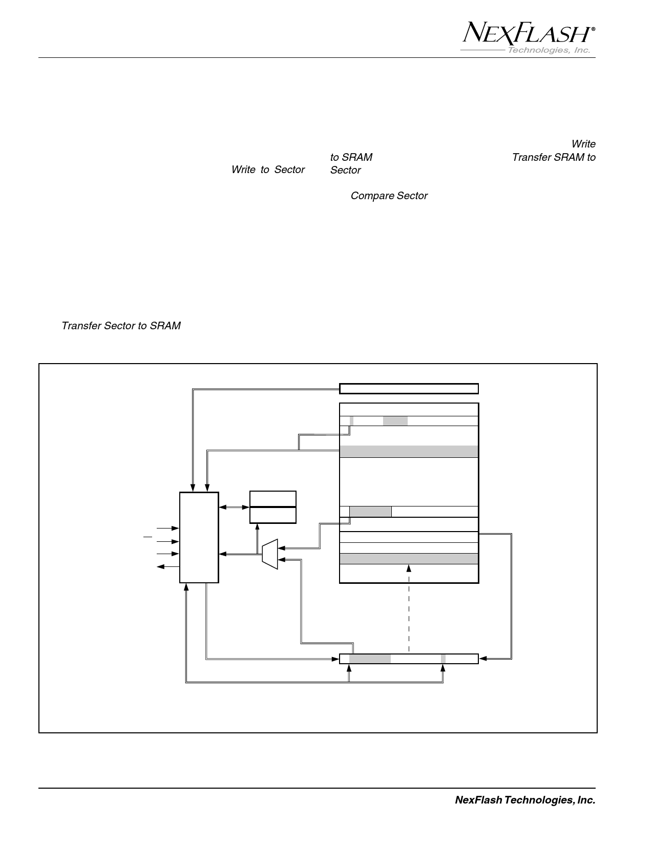
One of the most powerful features of the NX25F011B,
NX25F021B, and NX25F041B is the integrated Serial
SRAM. The main purpose of the Serial SRAM is to serve
as the primary buffer for sector data to be written into the
Serial Flash memory array. Using the Write to Sector
command, data is first shifted into the SRAM from the SPI
bus. When the command sequence has been completed, the
entire 264-bytes is written to the selected sector. See
Erase/Write cycle timing (tWP).
The SRAM is fully byte-addressable. Thus, the entire
264-bytes, a single byte, or a sequence of bytes can be read
from, or written to the SRAM. This allows the SRAM to be
used as a temporary work area for read-modify-write
operations prior to a sector write.
The Transfer Sector to SRAM command allows the con-
tents of a specified sector of Flash memory to be moved to
the SRAM. This can be useful when only a portion of a sector
needs to be altered. In this case the sector is first transferred
to the SRAM, where modifications are made using the Write
to SRAM command. Once complete, a Transfer SRAM to
Sector command is used to update the sector.
The Compare Sector command allows the contents of the
SRAM to be compared with the specified sector in memory.
The result of the compare is set in the status register. This
command is useful for performing a fast verify of the last
sector write operation (see Write/ Verify Flow towards the
end of this data sheet). This command can be useful when
re-writing multi-sector files that have only minor changes
from the previous write. If the new data in the SRAM is the
same as the previously written data, the sector write can
be skipped. Used in this way, the command saves time
that would have been used for re-programming. It also
extends the endurance of the Flash memory cells.
READ FROM
DEVICE INFORMATION
SECTOR
READ FROM
SECTOR
SCK
CS
SI
SO
SPI
COMMAND
AND
CONTROL
LOGIC
CONFIGURATION
REGISTER
STATUS
REGISTER
COMPARE SECTOR
TO SRAM
DEVICE INFORMATION SECTOR
SERIAL FLASH MEMORY ARRAY
512, 1024 AND 2048 BYTE-ADDRESSABLE
SECTORS OF 264-BYTES EACH
TRANSFER
SECTOR TO
SRAM
READ FROM
OR WRITE TO
SRAM
WRITE TO SECTOR
(VIA SRAM)
SERIAL SRAM
Note:
1. A single byte, several bytes, or all bytes of a Flash sector, the SRAM, or Program Buffer may be addressed.
2. All double lines represent implied connections or actions.
Figure 5. Command Relationships of the SPI Interface, Serial Flash Memory Array and SRAM
8
NexFlash Technologies, Inc.
PRELIMINARY NXSF016F-1201
12/12/01 ©
Share Link: 